Supercharge Your Innovation With Domain-Expert AI Agents!

Testing system and testing method for optoelectronic integrated circuit chip

A technology of integrated circuits and test systems, applied in the field of test systems for optoelectronic integrated circuit chips, can solve the problems of unstable test and long test time, and achieve the effects of reducing test costs, shortening test time, and enhancing stability

Active Publication Date: 2014-02-12
深圳米飞泰克科技股份有限公司
View PDF3 Cites 0 Cited by
  • Summary
  • Abstract
  • Description
  • Claims
  • Application Information

AI Technical Summary

Problems solved by technology

[0004] The purpose of the embodiments of the present invention is to provide a test system for optoelectronic integrated circuit chips, which aims to solve the problems of too long testing time and unstable testing of optoelectronic integrated circuit chips in the prior art

Method used


Image

  • Testing system and testing method for optoelectronic integrated circuit chip
  • Testing system and testing method for optoelectronic integrated circuit chip

Examples


Embodiment 1

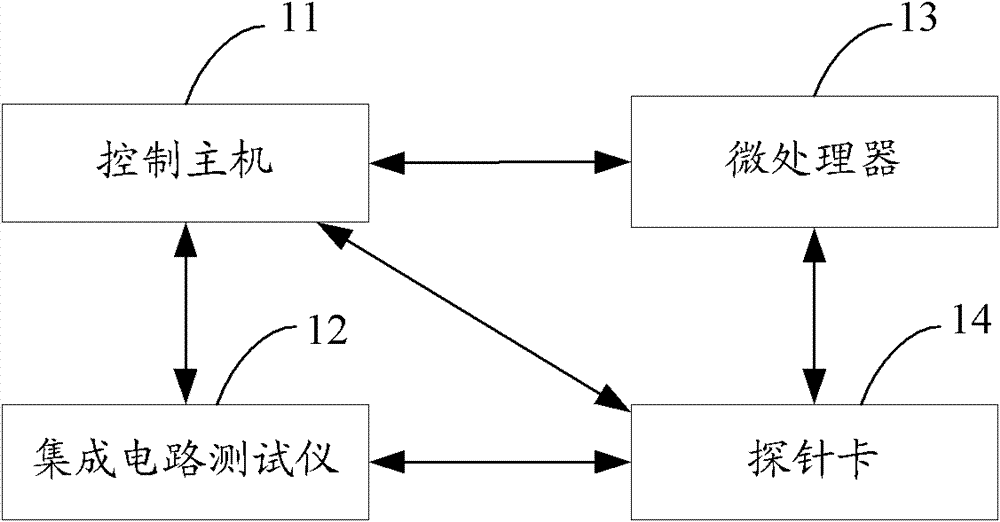
[0030] figure 1 The structure of the test system of the optoelectronic integrated circuit chip provided by the embodiment of the present invention is shown, and the details are as follows:

[0031] The test system of this optoelectronic integrated circuit comprises: control host computer 11, integrated circuit tester 12, with hardware internal integrated circuit bus 1 2 C or the microprocessor (MicroControl Unit, MCU) 13 of the system management bus SMBuS protocol module, and the probe card ProberCard 14 carrying the peripheral circuit of the chip to be tested.

[0032] The control host 11 is connected with the integrated circuit tester 12, MCU13, and Prober Card14, and is used to send the logic function parameters of the chip to be tested to the MCU13, and the MCU13 performs relevant logic on the chip to be tested connected to it according to the received logic function parameters. Functional test, after the test is completed, the logic function test result of the chip is se...

Embodiment 2

[0038] In the embodiment of the present invention, in order to save the logic function test result of the chip to be tested received by the control host 11, or to save the judgment result after the control host 11 judges the test result, a storage device can be set in the control host 11. The unit is used to store logic function test results or judgment results.

[0039] Since the storage unit stores the logic function test result sent by the MCU or the judgment result after making a judgment on the test result, the test result or judgment result can be extracted from the control host 11 very conveniently when the above test result or judgment result is used next time.

Embodiment 3

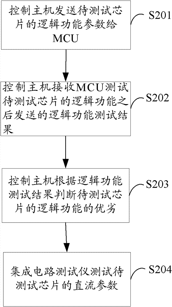
[0041] In the embodiment of the present invention, first, the control host 11 sends the logic function parameters of the chip to be tested to the MCU 13 connected to it through the RS-232 serial port. Then, MCU13 passes through I according to the logic function parameter that receives 2 C or the SMBuS protocol function to realize the relevant logic function test of the chip to be tested, and finally, the test result information is sent to the control host 11 by way of the RS-232 serial port.

[0042] In addition, the control host 11 is connected to the Prober Card 14 through the RS-232 interface, and controls the Prober Card 14 to complete the testing process of the entire chip.


PUM


Abstract

The invention is applicable to the field of testing, and provides a testing system and a testing method for an optoelectronic integrated circuit chip. The testing system comprises a master control unit, an integrated circuit tester, an MCU (micro-control unit) with a hardware I2C (inter-integrated circuit) bus or SM (system management) bus protocol module, and a probe card holding a peripheral circuit of a chip to be tested. The master control unit is connected with the integrated circuit tester, the probe card and the MCU, the MCU is connected with the probe card, and the integrated circuit tester is used for testing direct current parameters of the chip to be tested. When the testing system and the testing method are used for testing functions of optoelectronic integrated circuits, the MCU with the hardware I2C or SM bus protocol is used for testing functions of the chip, and accordingly testing time for the chip can be shortened effectively, testing stability can be enhanced, and overall testing cost is reduced.

Description

technical field [0001] The invention belongs to the field of circuit testing, in particular to a testing system and testing method for an optoelectronic integrated circuit chip. Background technique [0002] An optoelectronic integrated circuit is an integrated circuit that integrates an optical sensor on a semiconductor silicon chip. It is characterized in that the input optical analog signal is directly converted into a digital signal output, resulting in higher integration and better stability. The digital output signal of this type of chip mostly adopts the mode of serial bus protocol, such as the internal integrated circuit (Inter-Integrated Circuit, I 2 C) bus, system management bus (System ManagementBus, SMBuS), etc. The test method for this kind of integrated circuit chip is different from the traditional test method, which is mainly reflected in the test of the chip function. The traditional chip function test method is to use the test system to apply incentives t...

Claims


Application Information

Patent Timeline
Patent Type & Authority Patents(China)
IPC IPC(8): G01R31/28
Inventor 方盼李小明杨再林
Owner 深圳米飞泰克科技股份有限公司
Features
  • R&D
  • Intellectual Property
  • Life Sciences
  • Materials
  • Tech Scout
  • Unparalleled Data Quality
  • Higher Quality Content
  • 60% Fewer Hallucinations
Learn More