Manufacturing method for stepped silicon germanium source/drain structures

A manufacturing method and step-like technology, which are applied in semiconductor/solid-state device manufacturing, electrical components, circuits, etc., can solve the problems of poor etching selection, complex process steps, and difficult etching process control, and reduce etching steps. , The effect of high etching selection ratio and reducing control difficulty

Active Publication Date: 2013-10-23
SEMICONDUCTOR MANUFACTURING INTERNATIONAL (BEIJING) CORP +1
View PDF5 Cites 4 Cited by
  • Summary
  • Abstract
  • Description
  • Claims
  • Application Information

AI Technical Summary

Problems solved by technology

[0006] However, in the above-mentioned manufacturing methods of the stepped silicon germanium source / drain structure, the stepped recessed region is formed through a multi-step etching process, that is, a recessed portion is formed by one etching process first, and then another etching process is used to form a recessed portion. The process forms another depression, and the process steps are relatively complicated; and, when performing the above-mentioned multiple etching steps, the crystalline silicon body is etched, and the etching selection is relatively poor, and it is difficult to control the depth and depth of the formed depression. It is difficult to control the morphology and etching process

Method used


Image

  • Manufacturing method for stepped silicon germanium source/drain structures
  • Manufacturing method for stepped silicon germanium source/drain structures
  • Manufacturing method for stepped silicon germanium source/drain structures

Examples


Embodiment 1

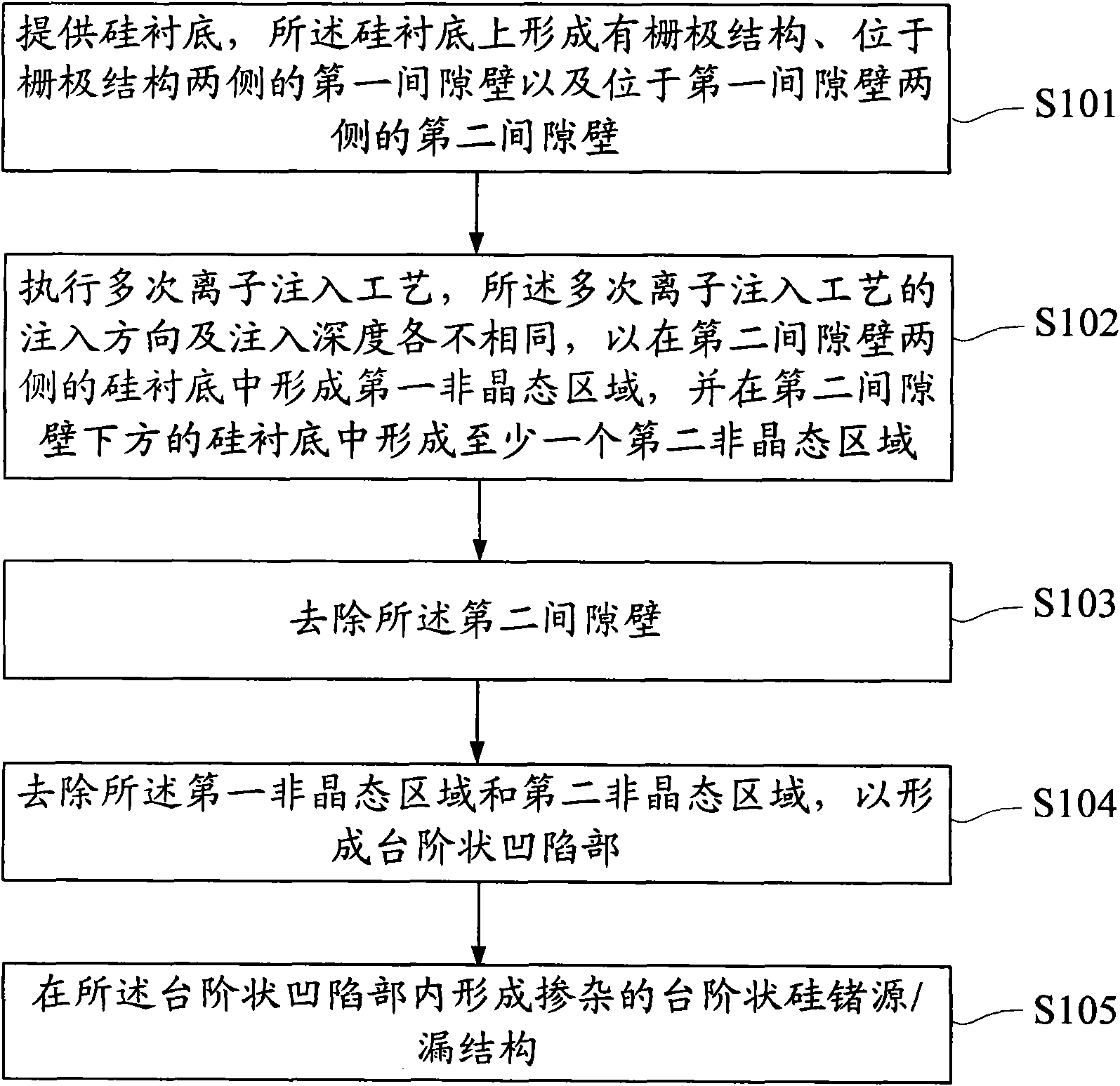
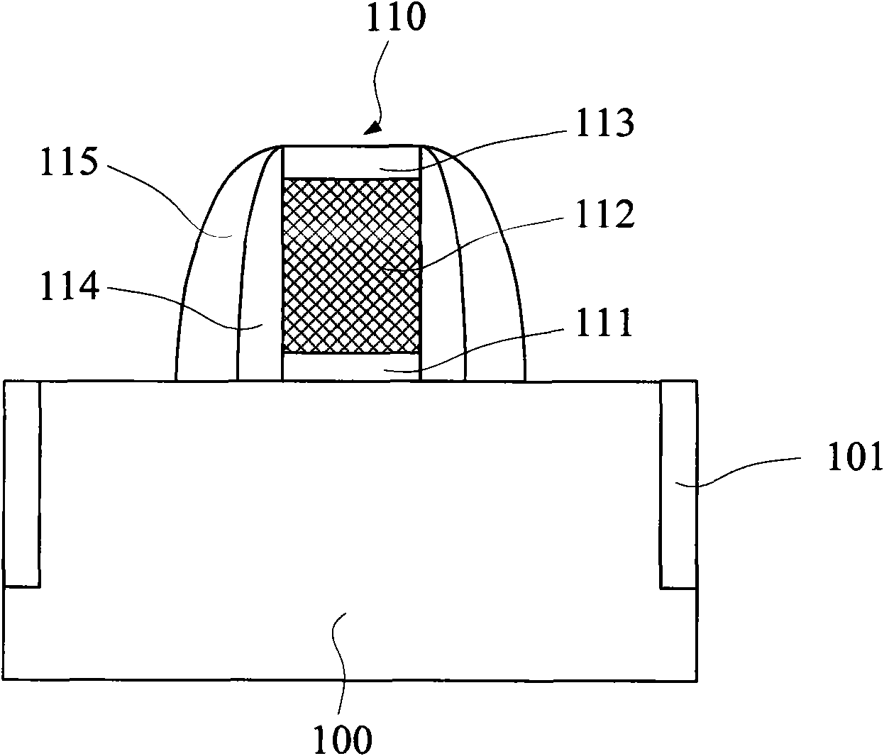
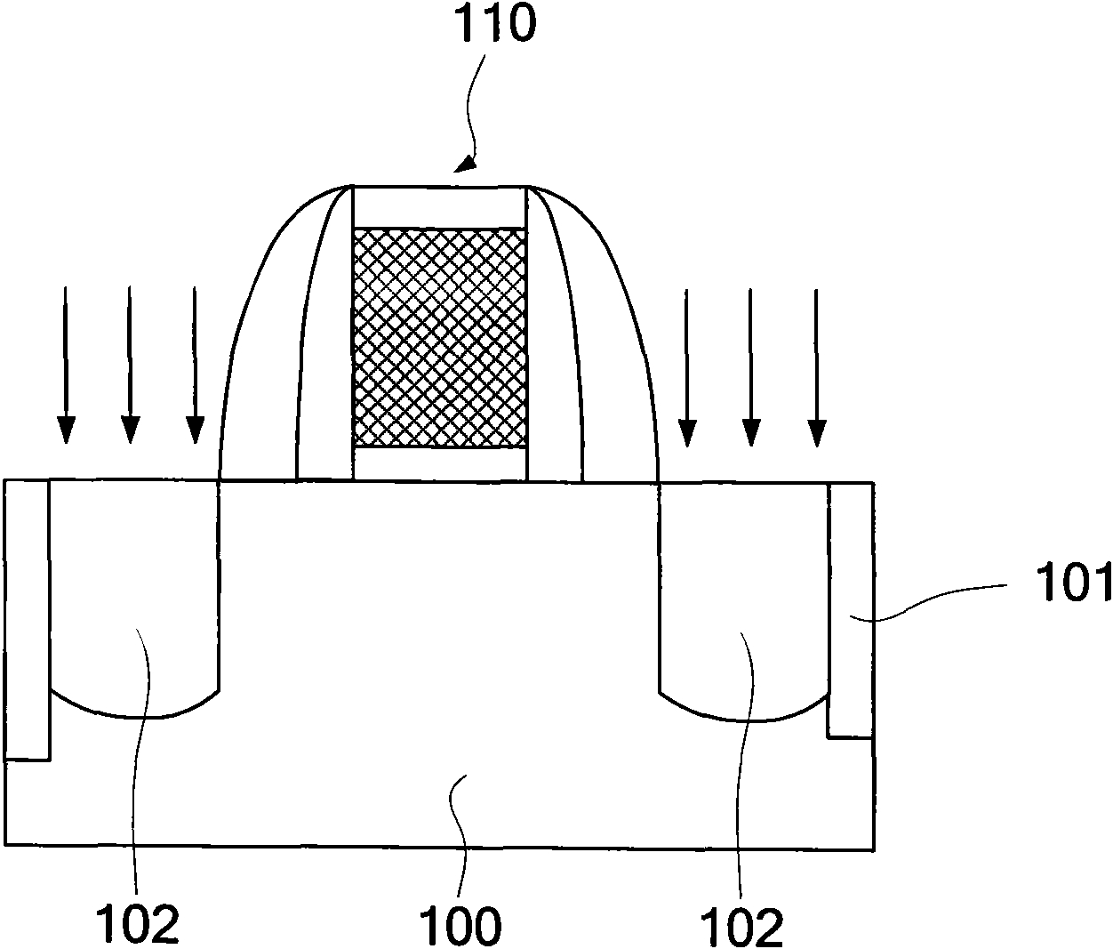
[0035] Such as Figure 2A As shown, and combined with step S101, first, a silicon substrate 100 is provided, and a gate structure 110 is formed on the silicon substrate 100, and then first spacers 114 are formed on both sides of the gate structure 110, and then Second spacers 115 are formed on both sides of the first spacer 114 .

[0036] Wherein, an isolation structure 101 may be formed in the silicon substrate 100, and the isolation structure 101 is, for example, a shallow trench isolation structure. The gate structure 110 includes a gate dielectric layer 111 and a gate electrode 112 covering the gate dielectric layer 111 . The material of the gate dielectric layer 111 may be silicon oxide, and the material of the gate electrode 112 may be doped polysilicon, metal, metal silicide or other conductors. Preferably, the gate structure 110 further includes a cover layer 113 covering the gate electrode 112, the material of the cover layer 113 can be one of silicon oxide or silic...

Embodiment 2

[0054] Such as Figure 3A As shown, a silicon substrate 200 is provided, and a gate structure 210 is formed on the silicon substrate 200, and then first spacers 214 are formed on both sides of the gate structure 210, and then on the first spacers 214 Second spacers 215 are formed on both sides, and an isolation structure 201 may be formed in the silicon substrate 200 .

[0055] The difference between this embodiment and Embodiment 1 is that in this embodiment, a total of three ion implantation processes are performed, wherein the angle between the implantation direction of the first ion implantation process and the surface of the silicon substrate 200 is a right angle, so that A first amorphous region is formed in the silicon substrate on both sides of the second spacer 215, and then a second ion implantation process and a third ion implantation process are performed, the second ion implantation process and the third ion implantation process The angle between the implantation...


PUM


Abstract

The invention provides a manufacturing method for stepped silicon germanium source / drain structures, which includes firstly, providing a silicon substrate, wherein a grid structure, first gap walls on two sides of the grid structure and second gap walls on two sides of each first gap wall are formed on the silicon substrate, secondly, performing multiple times of ion implantation technology by different directions and depths to form a first amorphous state region in the silicon substrate on two sides of each second gap wall and form at least one second amorphous state region in the silicon substrate below the second gap walls, thirdly, removing the second gap walls, fourthly, removing the first amorphous state regions and the second amorphous state regions to form a stepped recess, and fifthly, forming a doped stepped silicon germanium source / drain structure in the stepped recess. Compared with the prior art, the manufacturing method for stepped silicon germanium source / drain structures can reduce etching procedures and lower control difficulty of the etching process.

Description

technical field [0001] The invention relates to the field of integrated circuit manufacturing, in particular to a method for manufacturing a stepped silicon germanium source / drain structure. Background technique [0002] At present, the industry generally applies the selective epitaxial growth process of SiGe to the semiconductor process to increase carrier mobility and cost-effectiveness. Embedded silicon germanium (Embedded SiGe) technology has become a promising technology for producing silicon-based high-performance transistors. Since the radius of the germanium atom is larger than that of the silicon atom, when the germanium atom replaces part of the silicon atom and enters the silicon lattice, the entire lattice will be distorted. When the charge density of carriers is the same, compared with single crystal silicon, the mobility of electrons and holes in silicon or silicon germanium alloy with twisted lattice increases by about 5 and 10 times respectively. Can reduce...

Claims


Application Information

Patent Timeline
Patent Type & Authority Patents(China)
IPC IPC(8): H01L21/336H01L21/265
Inventor 李凤莲
Owner SEMICONDUCTOR MANUFACTURING INTERNATIONAL (BEIJING) CORP
Why Eureka
Try Eureka