Semiconductor device and method for fabricating semiconductor device

A semiconductor and component technology, applied in semiconductor/solid-state device manufacturing, semiconductor devices, semiconductor/solid-state device components, etc., can solve problems such as large silicon, improve reliability, increase pass rate, and increase production capacity.

Active Publication Date: 2012-04-04
TAIWAN SEMICON MFG CO LTD
View PDF6 Cites 20 Cited by
  • Summary
  • Abstract
  • Description
  • Claims
  • Application Information

AI Technical Summary

Problems solved by technology

For example, the PI layer requires a high temperature and long-term curing process (Curing Process), which leads to the shrinkage of the large volume of PI, which in turn produces a large residual (Residual) stress on the silicon.

Method used


Image

  • Semiconductor device and method for fabricating semiconductor device
  • Semiconductor device and method for fabricating semiconductor device
  • Semiconductor device and method for fabricating semiconductor device

Examples


Embodiment Construction

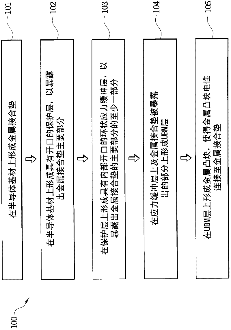
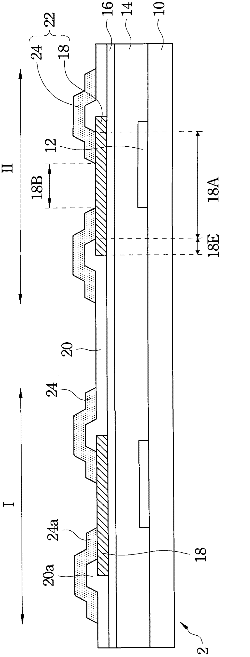
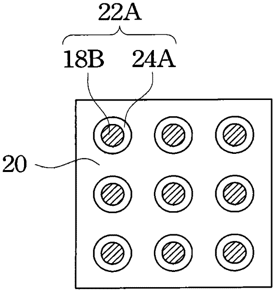
[0048] The invention provides a semiconductor component with a bonding pad structure and a process for forming the semiconductor component, wherein the bonding pad structure is provided with a stress buffer layer. The above-mentioned semiconductor components may have copper pillars, pillar protection (Passivation) interconnection lines, solder bumps, and / or through-silicon vias (TSVs) fabricated therein, wherein the semiconductor components may be applied to overlay Assembly, WLCSP, three-dimensional integrated circuit (3D-IC) stacking, and / or any advanced packaging technology field. A detailed description will be given below with reference to exemplary embodiments in the corresponding drawings. Wherever possible, the same reference numbers are used in the drawings and description to refer to the same or like parts. In the drawings, shapes and thicknesses may be exaggerated for clarity and convenience. The invention is to be directed in particular to components which form pa...


PUM

PropertyMeasurementUnit
thicknessaaaaaaaaaa
thicknessaaaaaaaaaa
thicknessaaaaaaaaaa

Abstract

The invention provides a semiconductor device and a method for fabricating the semiconductor device. The semiconductor device has a pad structure with a ring-shaped stress buffer layer between a metal pad and an under-bump metallization (UBM) layer. The stress buffer layer is formed of a dielectric layer with a dielectric constant less than 3.5, a polymer layer, or an aluminum layer. The stress buffer layer is a circular ring, a square ring, an octagonal ring, or any other geometric ring.

Description

technical field [0001] The present invention generally relates to a semiconductor device, and more particularly to a semiconductor device having a bond pad (Pad / Bond Pad) structure, wherein the bond pad structure is provided with a stress buffer (Stress Buffer) layer. Background technique [0002] Modern integrated circuits (ICs) are indeed made up of millions of active components such as transistors and capacitors. These components are initially separated from each other, but then are interconnected (Interconnected) together to form a functional circuit. Typical interconnection structures include lateral interconnections (such as metal lines (conductors)) and vertical interconnections (such as vias and contacts). Interconnects are increasingly determining the performance and density limits of today's ICs. On top of the interconnect structures, bonding pads are formed and exposed on the surface of individual chips. The electrical connection via the bonding pad is used to ...

Claims


Application Information

Patent Timeline
Patent Type & Authority Applications(China)
IPC IPC(8): H01L23/485H01L23/522H01L23/31H01L21/60H01L21/56
CPCH01L2224/05541H01L2224/05573H01L2224/05681H01L2224/05562H01L2924/0105H01L2924/01049H01L2924/01025H01L23/525H01L2924/13091H01L2924/01038H01L2224/13147H01L2224/0401H01L2224/05015H01L2224/1147H01L2224/05558H01L2224/13083H01L24/11H01L2924/01013H01L2224/94H01L2224/0235H01L2224/10126H01L2224/05559H01L2924/0103H01L2224/06131H01L24/00H01L2224/13155H01L2224/05187H01L2924/0104H01L2224/05166H01L2224/1145H01L2924/01033H01L2924/01074H01L2924/01078H01L2224/05022H01L2924/01073H01L2224/05012H01L2224/02126H01L2224/05687H01L2224/11462H01L2924/01023H01L2924/01046H01L2224/11464H01L2924/01082H01L2224/13164H01L2224/05027H01L2224/13109H01L2224/05014H01L2224/05666H01L2924/01019H01L2224/13144H01L2924/01029H01L2224/11849H01L2224/05008H01L2224/05181H01L2924/014H01L2924/01024H01L2224/05572H01L2224/05582H01L2224/05018H01L2224/0345H01L24/03H01L2224/11452H01L2924/01047H01L2924/01079H01L2224/1132H01L24/05H01L24/13H01L2224/13139H01L2224/05647H01L2224/11912H01L2224/05005H01L23/3114H01L2924/10253H01L2924/01075H01L2924/01012H01L23/3157H01L2224/13111H01L2924/1306H01L2924/1305H01L2924/00014H01L2924/14H01L2224/0361H01L2224/03912H01L2224/1308H01L2924/35H01L2924/3512H01L2924/35121H01L2224/02166H01L2224/03H01L2224/11H01L2924/04941H01L2924/04953H01L2924/01028H01L2924/01022H01L2924/01083H01L2924/01051H01L2924/00H01L2224/05552H01L2924/0001H01L23/48
Inventor 吴伟诚侯上勇郑心圃刘醇鸿邱志威史朝文
Owner TAIWAN SEMICON MFG CO LTD
Why Eureka
Try Eureka