Semiconductor packaging through metallic bonding and method for same

A packaging method and a technology of metal bonds, which are applied in semiconductor devices, semiconductor/solid-state device manufacturing, semiconductor/solid-state device components, etc., can solve the problems of reducing the utilization rate of chips in semiconductor packages.

Active Publication Date: 2012-04-04
ALPHA & OMEGA SEMICON LTD
View PDF5 Cites 9 Cited by
  • Summary
  • Abstract
  • Description
  • Claims
  • Application Information

AI Technical Summary

Problems solved by technology

This measure greatly reduces the utilization

Method used


Image

  • Semiconductor packaging through metallic bonding and method for same
  • Semiconductor packaging through metallic bonding and method for same
  • Semiconductor packaging through metallic bonding and method for same

Examples


Embodiment 1

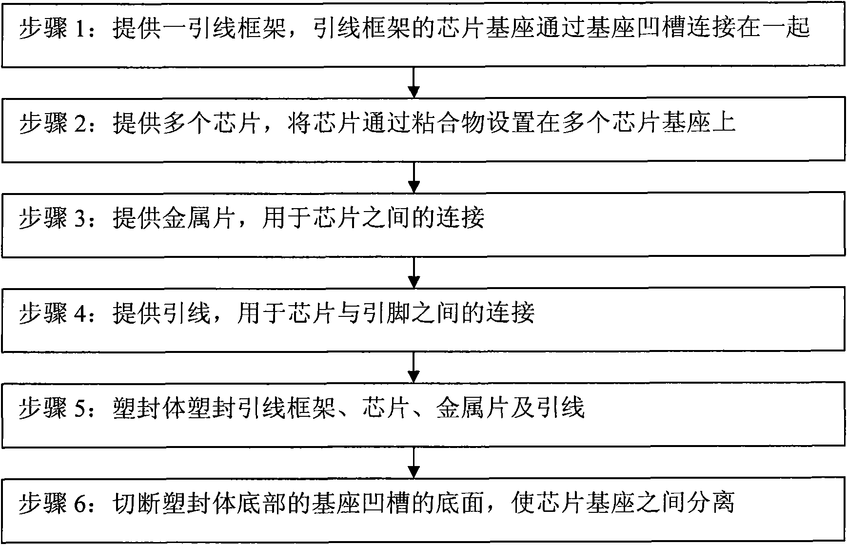
[0081] Embodiment 1: The present invention provides a metal sheet bonding packaging method. The packaging structure of the packaging method includes a lead frame 110, an adhesive 120, chips 130, 140, a metal sheet 150, a lead 160, and a plastic package 170. The flow chart of semiconductor packaging with metal sheet bonding is as follows: image 3 As shown, the specific encapsulation process is as follows:

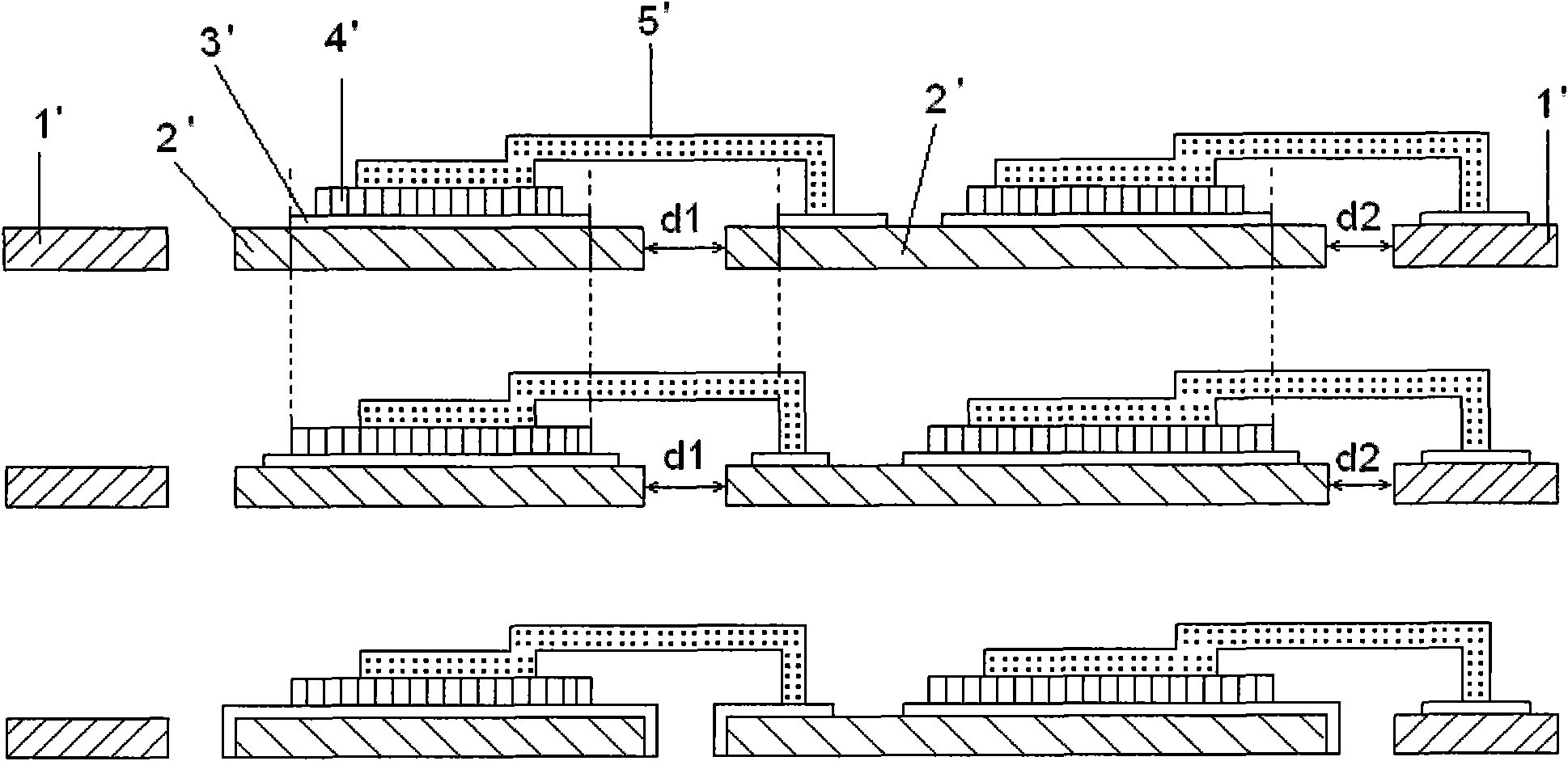
[0082] Such as Figure 4 As shown, firstly, a lead frame 110 is provided, and the lead frame 110 includes a chip base 115 and a plurality of pins. Figure 4 The upper figure is a top view of the lead frame, and the lower figure is a cross-sectional view along the dotted line in the previous figure. The chip base 115 includes a first chip mounting area 1151 , a second chip mounting area 1152 and a base groove 1153 . The base groove 1153 is disposed between the chip mounting areas and can distinguish each chip mounting area. In practical applications, multiple chip mountin...

Embodiment 2

[0089] Embodiment 2. The present invention provides a packaging method for metal sheet bonding. The packaging structure includes a lead frame 210, an adhesive 220, a chip 230, a metal sheet 240, a lead 250, and a plastic package 260. The semiconductor packaging method of the present invention Flowchart such as Figure 10 As shown, the specific packaging steps are as follows:

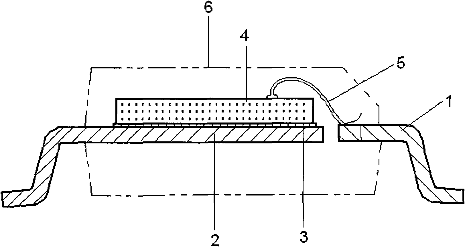
[0090] Such as Figure 11 As shown, a lead frame 210 is provided, and the lead frame 210 includes pins and a chip base 211 . The pins include two groups of pins 212 , 213 connected to the chip base 211 and arranged on both sides of the chip base 211 , and pins 214 disconnected from the chip base 211 . Such as figure 1 As shown, there is also a groove 215 between the base and the pins between the chip base 211 and the pins 213, and the groove 215 between the base and the pins separates the chip base 211 from the pins 213 Come.

[0091] Such as Figure 12 As shown, a chip 230 is provided, and the chi...

Embodiment 3

[0094] Embodiment 3. The above embodiment 1 is that the packaging structure connects each chip mounting area on the chip base before plastic sealing, and distinguishes them by base grooves. After the plastic sealing is completed, the base grooves are cut to complete the entire encapsulation process. The second embodiment is that the package structure connects the chip base and the pins together before plastic sealing, and distinguishes them by the groove between the base and the pins. After the plastic sealing is completed, the groove between the base and the pins is cut to complete the whole Encapsulation process. In a specific packaging process, Embodiment 1 and Embodiment 2 can be combined. Such as Figure 17 As shown, metal sheets are used instead of lead wires to connect the chip electrodes and pins, and the chip bases 311 in the lead frame 310 and between the chip bases 311 and the pins 312 are all connected together, and the base grooves 313 are respectively connected...


PUM


Abstract

The invention discloses a method for semiconductor packaging through metallic bonding, which is characterized in that the method includes the steps of firstly, providing a lead frame which comprises a chip substrate and pins, wherein the upper surface of the chip substrate is provided with at least one substrate groove which divides the whole chip substrate into a plurality of chip mounting areas, secondly, providing a plurality of chips which are all mounted in the corresponding chip mounting areas of the chip substrate through bonding, thirdly, providing at least one metallic sheet for connecting the chips, fourthly, providing leads for connecting the chips with the pins, fifthly, providing a plastic package body for packaging the structure, and sixthly, cutting off bottoms of the substrate grooves after packaging, so that the chip mounting areas in mutual connection are divided into disconnected chip mounting areas. The packaging method is capable of effectively preventing contamination caused by bonding overflowing during mounting of the chips to chip mounting equipment, the utilization ratio of the chips inside the package body is increased, and packaging cost is reduced.

Description

technical field [0001] The invention relates to a semiconductor package and a method thereof, in particular to a metal bonded semiconductor package and a method thereof. Background technique [0002] Packaging is very important to the chip. It not only protects the chip and enhances thermal conductivity, but also serves as a bridge between the internal world of the chip and the external circuit. At present, the continuous expansion of chip manufacturing scale and the huge and fast-growing terminal electronic application market have greatly promoted the growth of the entire semiconductor packaging industry. In order to meet the needs of light, thin, short, small products and initial system integration, various types of packaging structures have been introduced. Among them, wafer-level packaging that can meet the requirements of thin, light, short and high density has gradually attracted attention. [0003] Such as figure 1 As shown, the existing package includes a pin 1 , ...

Claims


Application Information

Patent Timeline
IPC IPC(8): H01L23/495H01L23/31H01L21/50H01L21/56
CPCH01L2224/32245H01L24/34H01L2224/73265H01L2924/00014H01L2224/48247H01L2224/48465H01L2924/13091H01L2924/1306H01L2224/40095H01L2924/181H01L2224/40245H01L24/40H01L2924/14H01L2224/48091H01L2224/73221H01L2224/371H01L2224/37H01L2224/40H01L2224/8385H01L2224/84801H01L2224/83801H01L2224/84385H01L2224/0603H01L2224/49111H01L2924/00H01L2224/45099H01L2924/00012
Inventor 薛彦迅安荷·叭剌鲁军
Owner ALPHA & OMEGA SEMICON LTD
Why Eureka
Try Eureka