MOS (metal oxide semiconductor) transistor

A MOS transistor and semiconductor technology, applied in semiconductor devices, electrical components, circuits, etc., can solve problems affecting the performance of transistors, achieve the effects of increasing device integration, improving performance, and reducing device size

Inactive Publication Date: 2012-04-04
CSMC TECH FAB1
View PDF2 Cites 10 Cited by
  • Summary
  • Abstract
  • Description
  • Claims
  • Application Information

AI Technical Summary

Problems solved by technology

Depend on figure 1 As shown, in this structure, the source metal layer 110 is located on the surface of the P-type well region 103, and the part in contact with the silicon body region is the lightly doped P-type well region 103, where the metal-semiconductor contact is easy to cause various Parasitic effects that affect transistor performance

Method used


Image

  • MOS (metal oxide semiconductor) transistor
  • MOS (metal oxide semiconductor) transistor
  • MOS (metal oxide semiconductor) transistor

Examples


Embodiment Construction

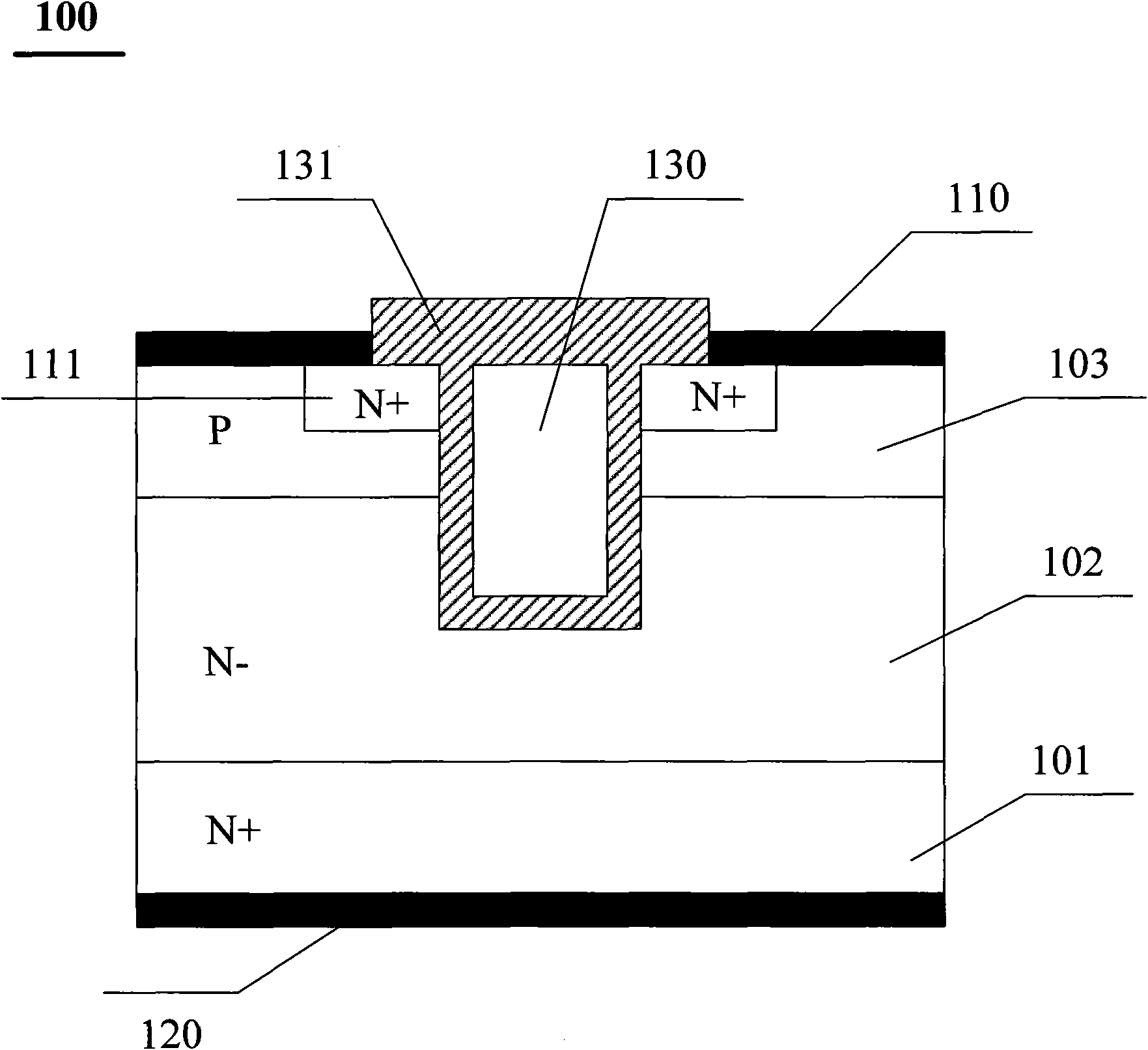
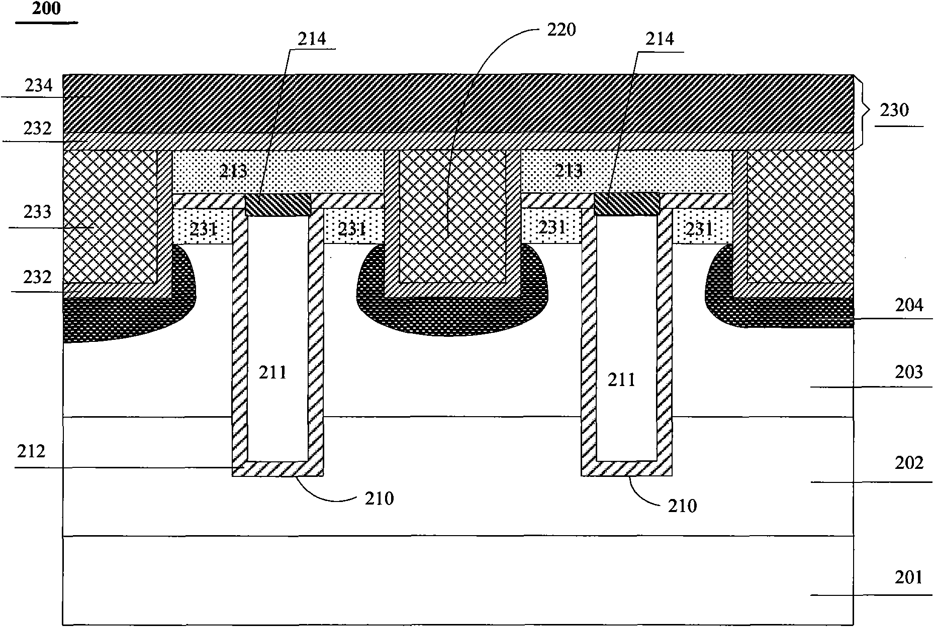
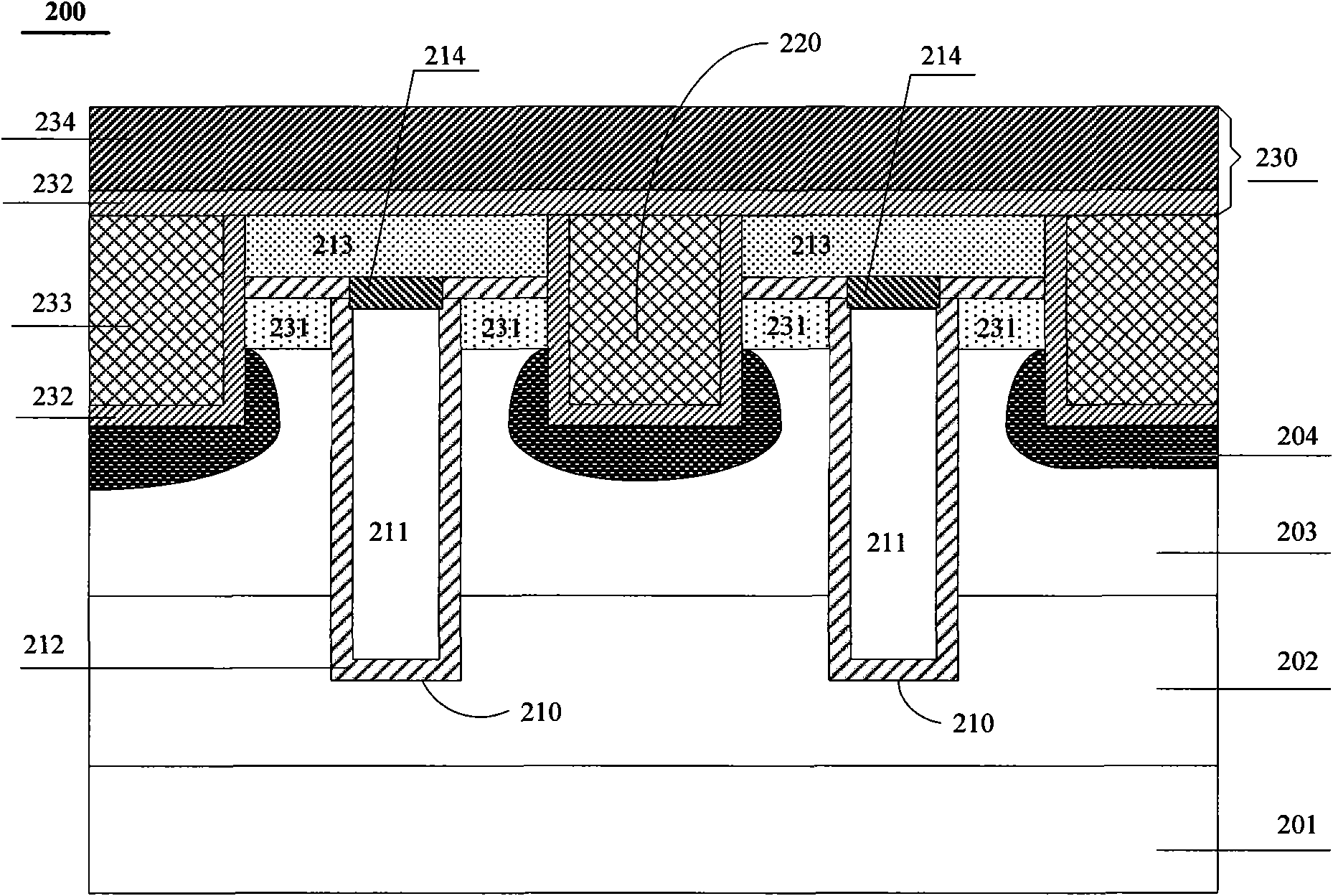
[0034] In order to make the object, technical solution and advantages of the present invention clearer, the present invention will be further described in detail below in conjunction with the accompanying drawings.

[0035] figure 2 A schematic diagram of the structure of the MOS transistor provided by the present invention.

[0036] like figure 2 As shown, the MOS transistor 200 is actually a trench-type vertical double-diffused transistor (TDMOS), and the TDMOS transistor 200 includes:

[0037] a semiconductor substrate 201 of a first semiconductor type;

[0038] an epitaxial layer 202 doped with the first semiconductor type located on the surface of the semiconductor substrate 201;

[0039] a well region 203 doped with a second semiconductor type located in the epitaxial layer 202;

[0040] A plurality of first trenches 210 located in the well region 203 have a trench depth greater than that of the well region 203 and extend into the epitaxial layer 202, and the first...


PUM


Abstract

The invention provides an MOS (metal oxide semiconductor) transistor, which is a trench vertical double-diffusion transistor. A metallic layer for leading a source electrode out is filled in a contact hole positioned between two adjacent source regions by means of a metallic plug, and a body contact area in heavy doping is formed below the contact hole. All metals in an MOS transistor structure pass through the metal plug filled in the contact hole to contact with a silicon body, the silicon body contacted by the side walls of the contact hole is a first semiconductor type doped source region, the silicon body contacted by the bottom of the contact hole is the second semiconductor type doped body contact area, and both the areas are heavy doped areas, so that various parasitic effects generated caused by contact of the metals with a light doped silicon body are prevented effectively, and the performance of the MOS transistor is improved. Simultaneously, by the aid of the metallic plug, the bore diameter of the contact hole is greatly reduced, the dimensions of devices are further decreased, and the integration level of the devices is improved.

Description

technical field [0001] The invention relates to a transistor structure, in particular to a trench type vertical double-diffusion transistor structure, which belongs to the technical field of semiconductors. Background technique [0002] In a semiconductor integrated circuit, a circuit based on a double-diffused MOS transistor, referred to as DMOS, uses the difference in the lateral diffusion speed of two impurity atoms to form a self-aligned sub-micron channel, which can achieve high operating frequency and speed. . [0003] Compared with ordinary MOS transistors, DMOS has two main differences in structure: one is that P-type and N-type impurities are sequentially diffused through the same oxide layer window to form a very short channel; A lightly doped N-drift region is added between them, whose doping concentration is much smaller than that of the channel region. This region bears most of the added drain voltage, thereby weakening the short channel effect and increasing ...

Claims


Application Information

Patent Timeline
Patent Type & Authority Applications(China)
IPC IPC(8): H01L29/78H01L29/36H01L29/08
CPCH01L29/66734H01L29/66727H01L29/456H01L29/1095H01L29/41766H01L29/7813
Inventor 王根毅吴宗宪
Owner CSMC TECH FAB1
Why Eureka
Try Eureka