
Semiconductor device

A semiconductor, conductive type technology, applied in the direction of semiconductor devices, electrical components, diodes, etc., can solve problems such as damage tolerance, reduction, and increase in hole discharge resistance.

Inactive Publication Date: 2014-11-05
KK TOSHIBA
View PDF6 Cites 0 Cited by
  • Summary
  • Abstract
  • Description
  • Claims
  • Application Information

AI Technical Summary

Problems solved by technology

However, if the trench spacing is narrowed, the area of ​​the P-type substrate layer that contacts the source electrode between the trenches becomes smaller.
This will lead to an increase in the discharge resistance of holes during avalanche breakdown, that is, a decrease in damage resistance.

Method used


Image

  • Semiconductor device
  • Semiconductor device
  • Semiconductor device

Examples


no. 1 approach

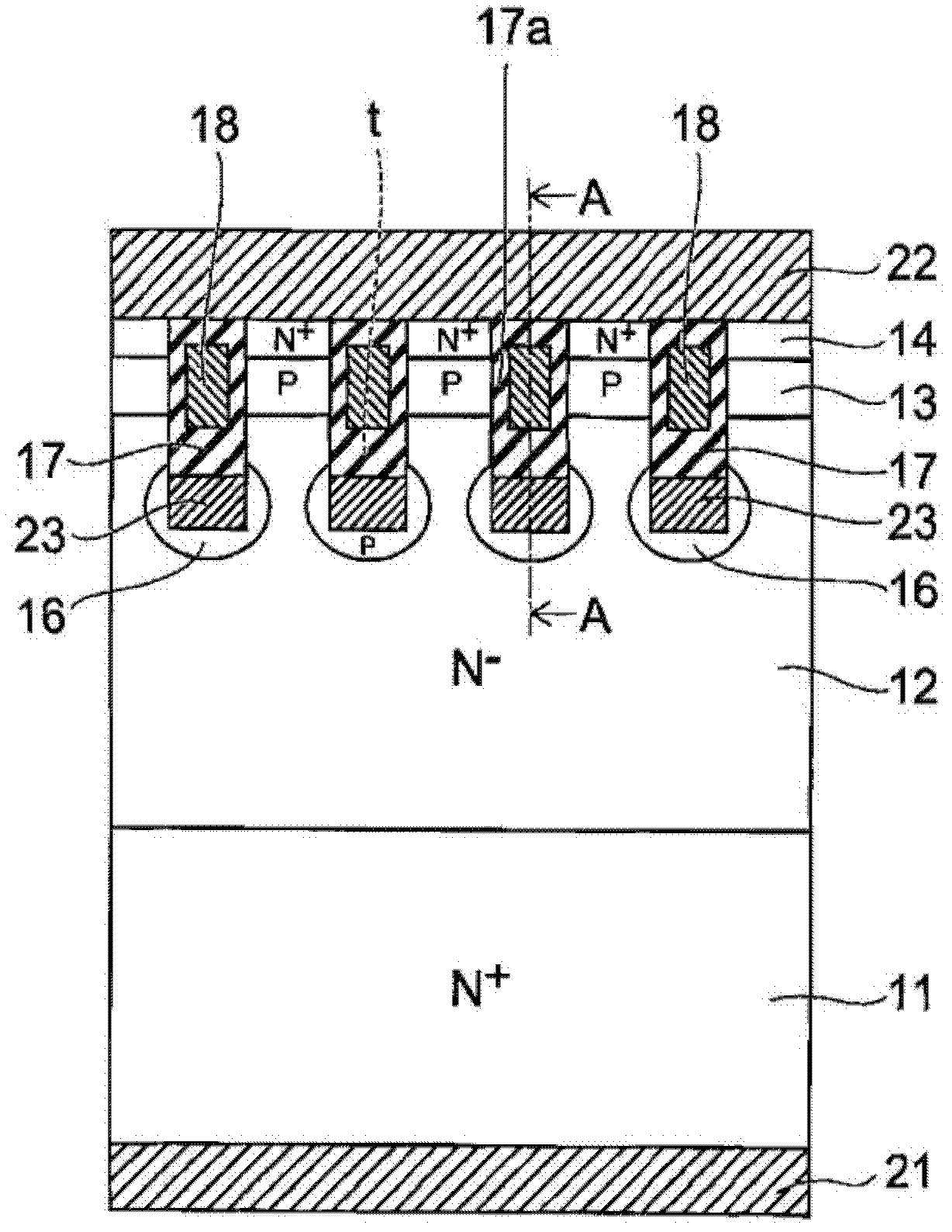
[0022] figure 1 It is a schematic cross-sectional view of the semiconductor device of the first embodiment.

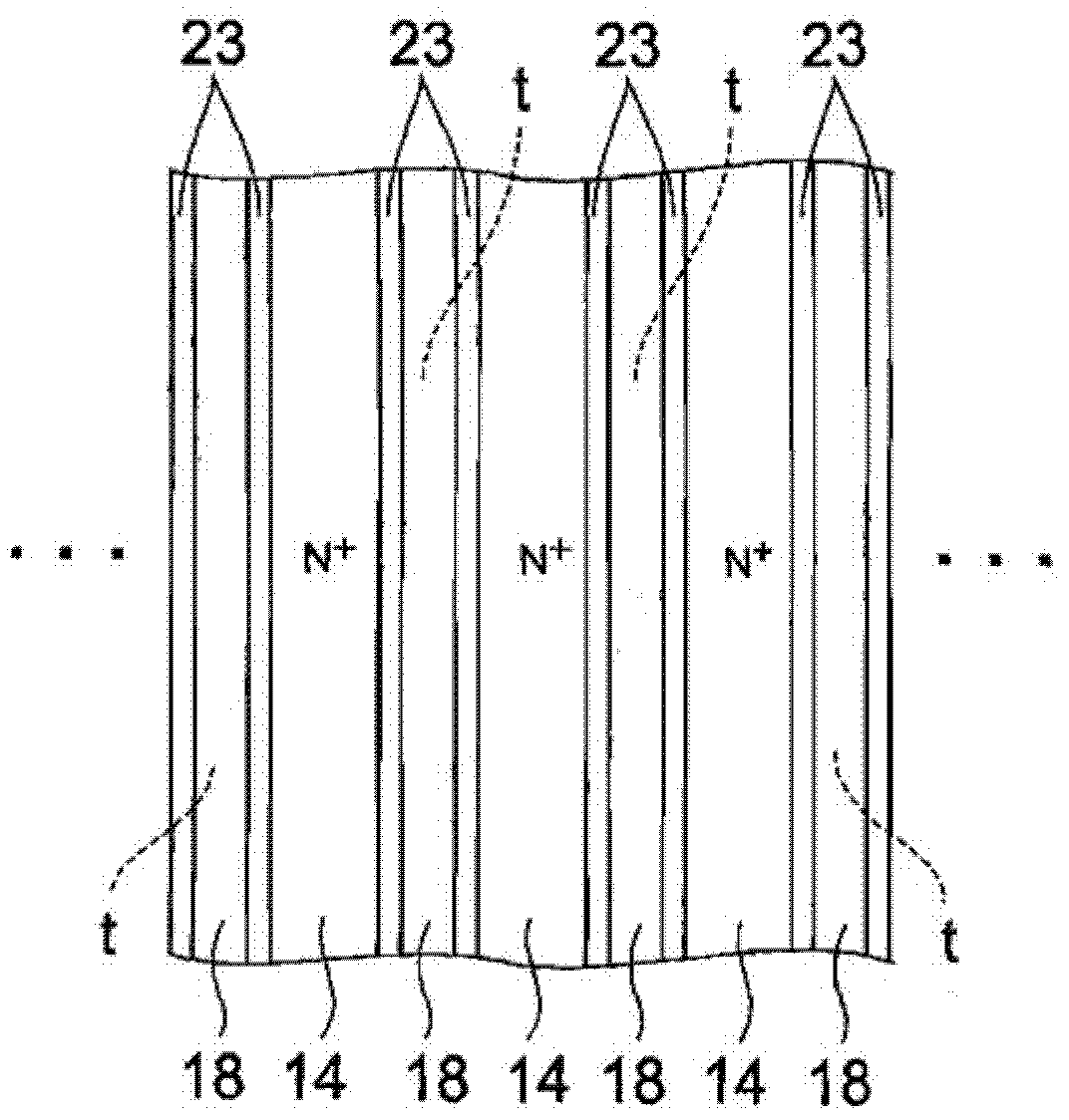
[0023] figure 2 is a schematic diagram illustrating a planar layout of main elements of the semiconductor device.

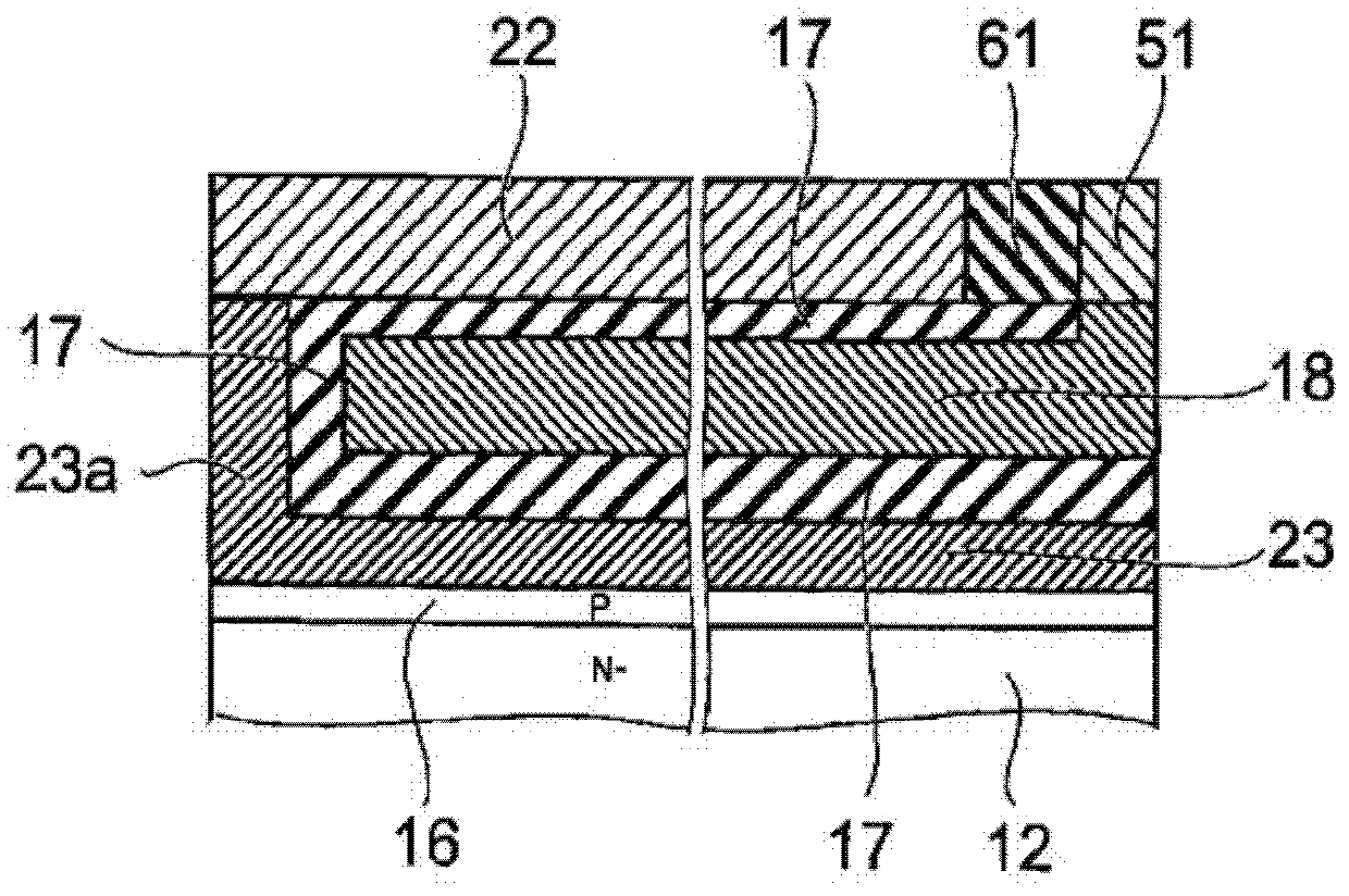
[0024] image 3 yes figure 1 A-A cutaway view.

[0025] The semiconductor layer includes N + Type drain layer 11, N - Type substrate layer 12, P type substrate layer 13, N + Type source layer 14 and P type buried layer 16. N + type drain layer 11 and N + type source layer 14 with N - The N-type substrate layer 12 has a higher concentration of impurities than the N-type.

[0026] N - type substrate layer 12 set in N + type drain layer 11. The P-type substrate layer 13 is set on the N - Type substrate layer 12. N + The P-type source layer 14 is disposed on the P-type substrate layer 13 . P-type buried layer 16 in N - In the type substrate layer 12, a plurality of them are selectively provided.

[0027] A plurality of trenches t are form...

no. 2 approach

[0053] Such as Figure 4 As shown, the buried electrode 23 may not be provided in all the trenches. exist Figure 4 In , a plurality of trenches are divided into a first trench t1 and a second trench t2 to show.

[0054] The first trench t1 from N + The surface of the P-type source layer 14 penetrates the P-type substrate layer 13 and reaches the N-type - Type substrate layer 12. An insulating film 17 is formed on the bottom surface and sidewalls of the first trench t. A gate electrode 18 is buried inside the insulating film 17 . The gate electrode 18 faces the P-type underlayer 13 via the gate insulating film 17 a formed on the sidewall of the first trench t1 .

[0055] The second trench t2 is also, from N + The surface of the source layer 14 passes through the P-type substrate layer 13 to reach the N-type substrate layer 12 . The second trench t2 is deeper than the first trench t1.

[0056] in N - A P-type buried layer 16 is selectively provided in the P-type subst...

no. 3 approach

[0069] then, Figure 5 It is a schematic cross-sectional view of the semiconductor device of the third embodiment.

[0070] In this embodiment, the P-type buried layer 16 and the buried electrode 33 are not provided in all the trenches. exist Figure 5 In , a plurality of trenches are divided into a first trench t1 and a second trench t3 to represent.

[0071] The first trench t1 from N + The surface of the P-type source layer 14 penetrates the P-type substrate layer 13 and reaches the N-type - Type substrate layer 12. An insulating film 17 is formed on the bottom surface and sidewalls of the first trench t. A gate electrode 18 is buried inside the insulating film 17 . The gate electrode 18 faces the P-type underlayer 13 via the gate insulating film 17 a formed on the sidewall of the first trench t1 .

[0072] The second trench t3 also starts from N + The surface of the P-type source layer 14 penetrates the P-type substrate layer 13 and reaches the N-type - Type subst...


PUM


Abstract

According to one embodiment, a semiconductor device includes a first major electrode, a first semiconductor layer, a first conductivity-type base layer, a second conductivity-type base layer, a second semiconductor layer, a buried layer, a buried electrode, a gate insulating film, a gate electrode, and a second major electrode. The buried layer of the second conductivity type selectively is provided in the first conductivity-type base layer. The buried electrode is provided in a bottom portion of a trench which penetrates the second conductivity-type base layer to reach the buried layer. The buried electrode is in contact with the buried layer. The gate electrode is provided inside the gate insulating film in the trench. The second major electrode is provided on the second semiconductor layer and is electrically connected to the second semiconductor layer and the buried electrode.

Description

[0001] This application is based on and enjoys priority from Japanese Patent Application No. 2010-206379 filed on September 15, 2010, the entire content of which is incorporated by reference. technical field [0002] The present invention relates to a semiconductor device. Background technique [0003] As a power device, for example, a vertical MOSFET (Metal-Oxide-Semiconductor Field Effect Transistor: Metal-Oxide-Semiconductor Field Effect Transistor) having a trench gate structure is widely used. For example, in the N-channel type, if a positive bias is applied to the gate electrode, an N-channel is formed near the boundary surface of the P-type substrate layer and the gate insulating film, and electrons pass through the N-channel and N-type substrate layers from the source layer. And the drain layer flows to the drain electrode, and becomes a conduction state. [0004] In this structure, if the trench interval is narrowed, the channel density will increase and the on-res...

Claims


Application Information

Patent Timeline
Patent Type & Authority Patents(China)
IPC IPC(8): H01L29/78H01L29/739H01L29/10
CPCH01L29/41766H01L29/7805H01L29/7813H01L29/0696H01L29/41741H01L29/1095H01L29/7397H01L29/66348H01L29/42356H01L29/7831
Inventor 小仓常雄
Owner KK TOSHIBA
Learn More