Plasma etching method, device thereof and plasma etching method for diffusion barrier layers

An etching device, plasma technology, applied in the direction of plasma, discharge tube, electrical components, etc., can solve the problems of reliability, inconsistent thickness of diffusion barrier layer, difference in resistance of metal interconnection structure, etc., to achieve consistent etching rate, Improved thickness uniformity, uniform plasma gas distribution

Active Publication Date: 2013-10-09
SEMICON MFG INT (SHANGHAI) CORP +1
View PDF1 Cites 0 Cited by
  • Summary
  • Abstract
  • Description
  • Claims
  • Application Information

AI Technical Summary

Problems solved by technology

[0011] The purpose of the present invention is to provide a plasma etching method and its device, which are applied to the manufacture of diffusion barrier layers, so as to solve the problem of inconsistency in the thickness of the diffusion barrier layer caused by the difference in etching rates in various places on the semiconductor wafer, which in turn leads to metal interconnection. Differences in the resistance of various parts of the structure, resulting in product reliability problems

Method used


Image

  • Plasma etching method, device thereof and plasma etching method for diffusion barrier layers
  • Plasma etching method, device thereof and plasma etching method for diffusion barrier layers
  • Plasma etching method, device thereof and plasma etching method for diffusion barrier layers

Examples


Embodiment Construction

[0036] In order to make the above objects, features and advantages of the present invention more comprehensible, specific implementations of the present invention will be described in detail below in conjunction with the accompanying drawings.

[0037] In the following description, many specific details are set forth in order to fully understand the present invention, but the present invention can also be implemented in other ways than those described here, so the present invention is not limited by the specific embodiments disclosed below.

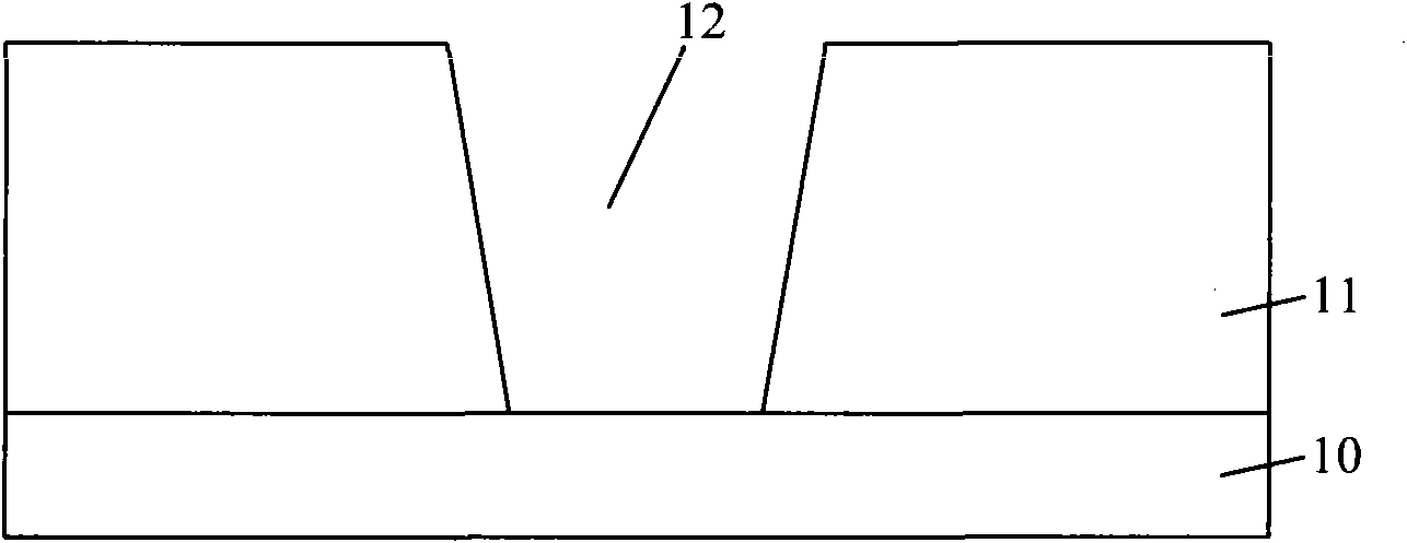
[0038] As mentioned in the background technology section, due to the limitation of the plasma etching process in the prior art, the etching rate of the diffusion barrier layer on the surface of the wafer is different, resulting in inconsistent thickness of the diffusion barrier layer after thinning, which makes the subsequent fabrication There are large resistance differences throughout the metal interconnection structure, which affects th...


PUM


Abstract

The invention provides a plasma etching method, a device thereof and a specific method applying the device to carry out plasma etching on diffusion barrier layers, wherein the plasma etching method includes the following steps: an outer electrode collar and an inner electrode collar are concentrically arranged in an etching chamber; a semiconductor wafer to be etched is arranged on the bottoms of the outer electrode collar and the inner electrode collar, and the center of the semiconductor wafer is superposed with the circle center of the outer electrode collar and the inner electrode collar; etching gas is filled into the etching chamber; the outer electrode collar and the inner electrode collar are electrified, and the current directions of the outer electrode collar and the inner electrode collar are opposite. The invention ensures that the distribution of the plasma gas of the surface of the semiconductor wafer is uniform and the etching rate at each position is equal, thus improving the thickness consistency of each diffusion barrier layer at each position on the semiconductor wafer.

Description

technical field [0001] The present invention relates to the technical field of semiconductors, and more specifically, the present invention relates to a plasma etching method and device thereof, and a plasma etching method of a diffusion barrier layer. Background technique [0002] In the metal interconnection process, interconnection metals such as copper, aluminum or tungsten need to be filled in the interconnection structure (including trenches, contact holes, etc.). In order to prevent the above-mentioned metals from diffusing into the surrounding insulating dielectric layer, causing the insulation performance of the dielectric layer to decrease, and further generating leakage current, it is necessary to form a diffusion barrier layer on the inner wall of the trench and contact hole before conducting conduction. metal filling. Conventional diffusion barrier materials include metals or alloys containing tantalum and titanium, which can be a single-layer metal layer or a ...

Claims


Application Information

Patent Timeline
Patent Type & Authority Patents(China)
IPC IPC(8): H01L21/3213H01L21/768H01J37/32H05H1/16
Inventor 聂佳相何伟业孔祥涛陈碧钦
Owner SEMICON MFG INT (SHANGHAI) CORP
Why Eureka
Try Eureka