Printed circuit board and manufacturing method thereof

A technology for printed circuit boards and dielectric substrates, applied in the fields of printed circuit manufacturing, printed circuits, printed circuit components, etc., can solve the problems of increased signal transmission loss, loss of green oil coating layer, and PCB pressing warpage And other issues

Inactive Publication Date: 2012-04-11
DATANG MOBILE COMM EQUIP CO LTD
View PDF5 Cites 11 Cited by
  • Summary
  • Abstract
  • Description
  • Claims
  • Application Information

AI Technical Summary

Problems solved by technology

[0007] Using conventional PCB stacking and process methods, the green oil coating layer will bring a certain loss to signal transmission. At the same time, as the signal transmission rate increases, the skin effect increases, and the signal transmission loss increases; use high-performance boards , using mixed pr...

Method used


Image

  • Printed circuit board and manufacturing method thereof
  • Printed circuit board and manufacturing method thereof
  • Printed circuit board and manufacturing method thereof

Examples


Embodiment Construction

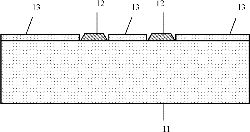
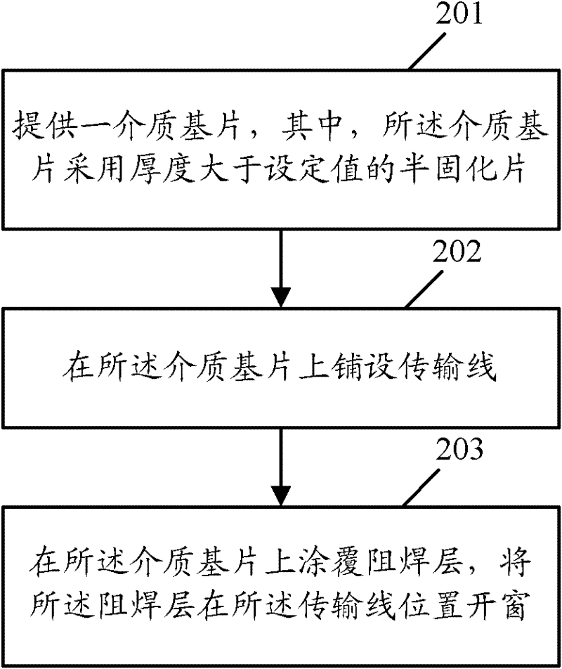
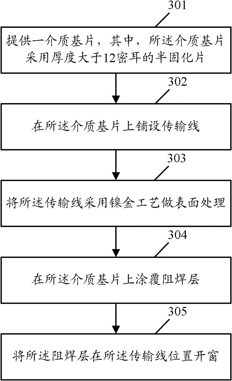
[0023] In order to reduce signal transmission loss and reduce production costs, the printed circuit board provided by the embodiment of the present invention includes: a dielectric substrate, using a prepreg with a thickness greater than a set value; a transmission line, formed on the dielectric substrate; A solder resist layer where the transmission line is windowed is formed on the dielectric substrate.

[0024] figure 1 It is a schematic structural diagram of a printed circuit board according to an embodiment of the present invention. Such as figure 1 As shown, the printed circuit board of the embodiment of the present invention includes:

[0025] The dielectric substrate 11 adopts a prepreg whose thickness is greater than a set value;

[0026] a transmission line 12 formed on the dielectric substrate 11;

[0027] A solder resist layer 13 with a window opened at the position of the transmission line 12 is formed on the dielectric substrate 11 .

[0028] The dielectric ...


PUM


Abstract

The invention discloses a printed circuit board and a manufacturing method thereof. The printed circuit board comprises a medium substrate and a transmission line, wherein the medium substrate is made of a prepreg with thickness larger than a set value, the transmission line is formed on the prepreg, a windowed solder mask is formed on the medium substrate at the position of the transmission line. By utilizing the technical scheme, the signal transmission loss can be reduced, the board cost can be reduced, the manufacturing process can be simplified and the production cost is lowered further.

Description

technical field [0001] The invention relates to the field of circuit boards, in particular to a printed circuit board and a manufacturing method thereof. Background technique [0002] With the rapid development of modern communication technology, the data transmission rate between boards is getting higher and higher, which has reached 10G bits per second, and the high-speed signal transmission has higher and higher requirements for signal quality. [0003] In modern communication circuit design, when signals are transmitted on a printed circuit board (Printed Circuit Board, PCB), the most commonly used structure of the transmission line is a microstrip line structure. The width and thickness of the signal transmission line, its distance from the ground plane, and the dielectric constant of the medium determine the characteristic impedance of the microstrip line. There are four most commonly used transmission line structures: surface microstrip line, embedded microstrip line...

Claims


Application Information

Patent Timeline
IPC IPC(8): H05K1/02H05K3/00
Inventor 李军刘爽郭东
Owner DATANG MOBILE COMM EQUIP CO LTD
Why Eureka
Try Eureka