Method for manufacturing insulated gate bipolar transistor (IGBT) device

A manufacturing method and device technology, applied in semiconductor/solid-state device manufacturing, electrical components, circuits, etc., can solve the problem of high cost, and achieve the effects of eliminating temperature limitations, high activation rate, and easy implementation

Active Publication Date: 2012-04-18
SHANGHAI HUAHONG GRACE SEMICON MFG CORP
View PDF6 Cites 31 Cited by
  • Summary
  • Abstract
  • Description
  • Claims
  • Application Information

AI Technical Summary

Problems solved by technology

However, the laser annealing process requires the...

Method used


Image

  • Method for manufacturing insulated gate bipolar transistor (IGBT) device
  • Method for manufacturing insulated gate bipolar transistor (IGBT) device
  • Method for manufacturing insulated gate bipolar transistor (IGBT) device

Examples


Embodiment Construction

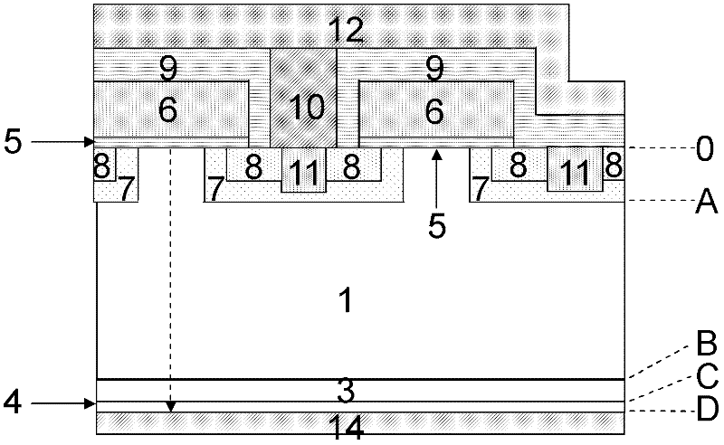
[0018] IGBT devices can be divided into three types: PT type (punch through), NPT type (non-punchthrough), and field stop type (field stop).

[0019] see figure 1 , which is a cross-sectional view of a field-stop IGBT device.

[0020] figure 1 The manufacturing method of the present invention of the shown field stop type IGBT device comprises the following steps:

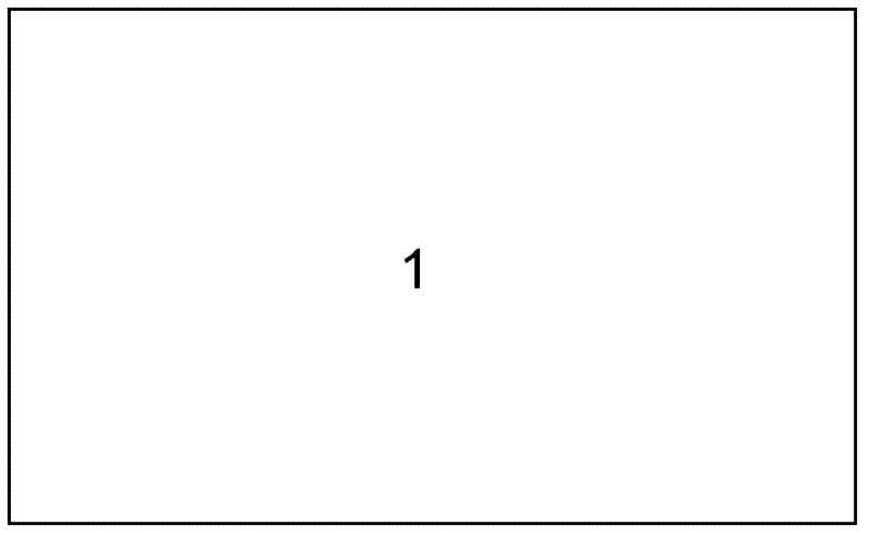
[0021] initial state, see Figure 2a , the thickness of the silicon wafer 1 is, for example, 700 μm, which is doped with n-type impurities, and the doping concentration is, for example, 2.4×10 13 atoms / cm 3 (atoms per cubic centimeter), the resistivity corresponding to this n-type doped silicon wafer 1 is, for example, 180Ω·cm (ohm·cm).

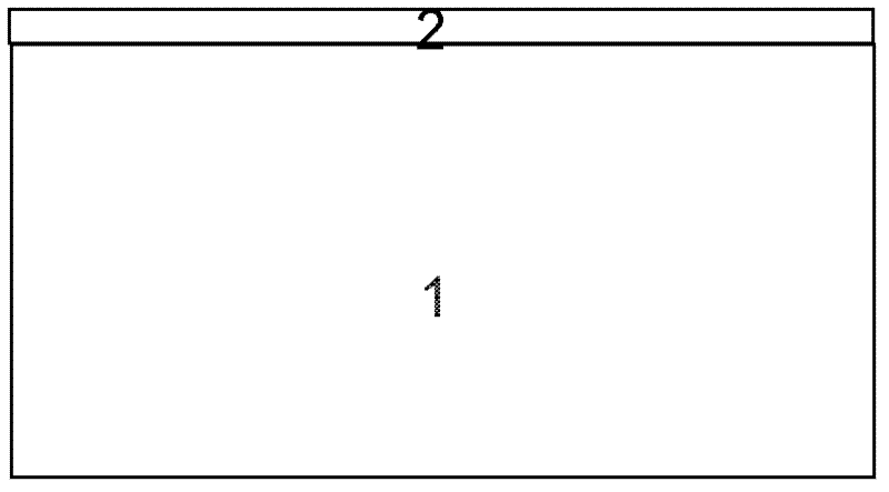
[0022] Step 1, see Figure 2b A layer of dielectric 2, such as silicon dioxide, is deposited on the front side of the silicon wafer 1 to protect the front side of the silicon wafer 1, and then the silicon wafer 1 is thinned from the back side. The thickness of the deposited ...


PUM

PropertyMeasurementUnit
Doping concentrationaaaaaaaaaa

Abstract

The invention discloses a method for manufacturing an insulated gate bipolar transistor (IGBT) device. The method sequentially comprises an ion injection step of forming a p type heavily doped collecting region on the back side of a silicon wafer, a partial or whole annealing step and a step of depositing surface metal on the front side of the silicon wafer; and after the p type heavily doped collecting region is formed on the back side of the silicon wafer, a layer of silicon dioxide is deposited on the back side of the p type heavily doped collecting region. The method has the advantages that the temperature limitation of the p type ion annealing on the back side of the silicon wafer is eliminated, and high activity rate is easy to obtain. Simultaneously, the p type impurity distribution in the p type heavily doped collecting region can be optimized. On one hand, the ohmic contact with back metal is easy to form, on the other hand, the emission efficiency of a precision navigation processor (PNP) is favorably controlled, and the alternating current characteristic of the IGBT device is improved.

Description

technical field [0001] The present invention relates to a power semiconductor device, in particular to an IGBT (Insulated Gate Bipolar Transistor, insulated gate bipolar transistor) device. Background technique [0002] The VDMOS (Vertical double diffused MOSFET, vertical double diffused MOS transistor) device is an n-type heavily doped region under its drift region (n-type medium and low doped region). If the n-type heavily doped region is changed to a p-type heavily doped region, and part of the n-type medium and low doped region (drift region) is not depleted when the device reverse breakdown occurs, an NPT is formed type IGBT devices. If the thickness of the n-type low-doped region (drift region) of the NPT-type IGBT device is thinned, all the n-type low-doped regions (drift region) are depleted when the reverse breakdown of the device occurs, and in An n-type layer with a higher doping concentration than the n-type low-doped region (drift region) is inserted between t...

Claims


Application Information

Patent Timeline
IPC IPC(8): H01L21/331H01L21/265
Inventor 肖胜安王海军刘坤
Owner SHANGHAI HUAHONG GRACE SEMICON MFG CORP
Why Eureka
Try Eureka