Method for improving reliability of under-gate technology high-K gate dielectric medium CMOS (complementary metal oxide semiconductor)

A gate-last process and gate dielectric technology are applied in the field of improving NMOS hot carrier effect and PMOS negative bias temperature instability effect to achieve the effect of improving reliability and improving performance

Active Publication Date: 2012-04-18
SHANGHAI HUALI MICROELECTRONICS CORP
View PDF3 Cites 6 Cited by
  • Summary
  • Abstract
  • Description
  • Claims
  • Application Information

AI Technical Summary

Problems solved by technology

Therefore, it is not enough to improve the HCI effect simp

Method used


Image

  • Method for improving reliability of under-gate technology high-K gate dielectric medium CMOS (complementary metal oxide semiconductor)
  • Method for improving reliability of under-gate technology high-K gate dielectric medium CMOS (complementary metal oxide semiconductor)
  • Method for improving reliability of under-gate technology high-K gate dielectric medium CMOS (complementary metal oxide semiconductor)

Examples


Embodiment Construction

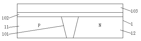
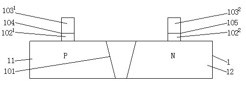
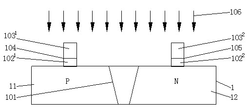
[0023] see Figure 1a As shown in -g, a method for improving the reliability of gate-last process high-K gate dielectric CMOS of the present invention, wherein, comprises the following steps:

[0024] A first dielectric layer 102 and a polysilicon layer 103 are sequentially deposited on the substrate 1, wherein the substrate 1 is provided with an isolation groove 101, and its two sides are respectively a P-type substrate 11 and an N-type substrate 12; using photolithography and Etching process, etching polysilicon layer 102 and first dielectric layer 103 to form NMOS semiconductor device sample gate 104 and PMOS semiconductor device sample gate 105, wherein, NMOS semiconductor device sample gate 104 is formed by first dielectric layer 102 1 and polysilicon layer 103 1 Composition, PMOS semiconductor device sample gate 105 is made of the first dielectric layer 102 2 and polysilicon layer 103 2 Composition: fluorine ions are implanted in the drain source region 114 by ion impl...


PUM


Abstract

The invention generally relates to a method for improving an NMOS (N-channel metal oxide semiconductor) hot carrier injection effect and a PMOS (P-channel metal oxide semiconductor) negative bias temperature instability effect in the field of semiconductor manufacturing, and in particular relates to a method for improving the NMOS hot carrier injection effect and PMOS negative bias temperature instability effect of an under-gate-technology high-K gate dielectric medium CMOS (complementary metal oxide semiconductor). The invention discloses a method for improving the reliability of the high-K gate dielectric medium CMOS in the under-gate-technology. According to the invention, in the under-gate technology manufacture process, fluorine ions are injected in NMOS and PMOS device regions through an ion injection process after a sample gate is formed, and a stable chemical bond is formed at the interface by virtue of a thermal treatment process, thereby effectively improving the HCI (hot carrier injection) effect resistance performance of the NMOS device and the NBTI (negative bias temperature instability) effect resistance performance of the PMOS device.

Description

technical field [0001] The present invention generally relates to a method for improving NMOS hot carrier effect and PMOS negative bias temperature instability effect in the field of semiconductor manufacturing. The method of NMOS hot carrier effect and PMOS negative bias temperature instability effect. Background technique [0002] In order to reduce gate leakage current and improve device performance, high-K gate dielectric technology has been applied to nodes below 45 nanometers; however, since the interface between high-K gate dielectric and silicon has a large number of interface states, and these interface states cannot It will form unstable hydrogen bonds with hydrogen, resulting in a large number of interface states during the operation of NMOS and PMOS devices, thereby changing the performance of MOS; that is, NMOS devices with high K gate dielectrics have very serious hot carrier (Hot Carrier Injection, referred to as HCI) effect, and PMOS devices have serious neg...

Claims


Application Information

Patent Timeline
IPC IPC(8): H01L21/8238
Inventor 谢欣云陈玉文
Owner SHANGHAI HUALI MICROELECTRONICS CORP
Why Eureka
Try Eureka