
Semiconductor chip and lead frame

A lead frame and semiconductor technology, applied in semiconductor devices, semiconductor/solid-state device components, electric solid-state devices, etc., can solve the problems of crystal and chip coordination error, low integration, large area occupied by circuits, etc., to improve Work stability, ensure consistency, and low chip cost

Inactive Publication Date: 2012-04-25
RFDOT MICROELECTRONICS +1
View PDF4 Cites 1 Cited by
  • Summary
  • Abstract
  • Description
  • Claims
  • Application Information

AI Technical Summary

Problems solved by technology

Existing chips are generally installed on a circuit board, and the clock frequency is provided by an external crystal oscillator, but such a chip provided by an external crystal oscillator will occupy a certain amount of space, and the area occupied by the entire circuit is relatively large. , the integration level is not high, and secondly, because the crystal and the chip are separated, the working environment will always be different, so that there will be errors in the cooperation between the crystal and the chip, which will affect the stability of the chip

Method used


Image

  • Semiconductor chip and lead frame
  • Semiconductor chip and lead frame
  • Semiconductor chip and lead frame

Examples


Embodiment Construction

[0015] Reference herein to "one embodiment" or "an embodiment" refers to a particular feature, structure or characteristic that can be included in at least one implementation of the present invention. "In one embodiment" appearing in different places in this specification does not all refer to the same embodiment, nor is it a separate or selective embodiment that is mutually exclusive with other embodiments.

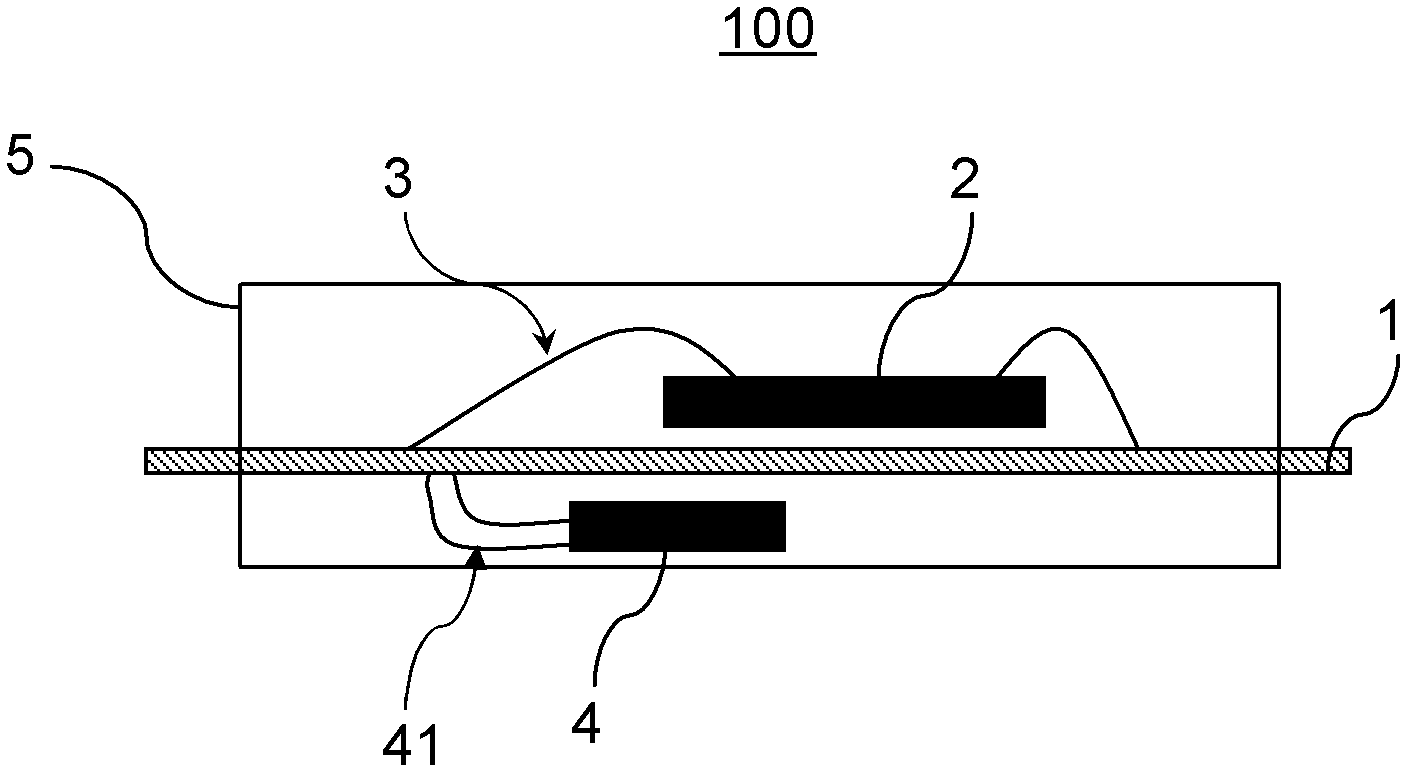
[0016] see figure 1 As shown, it shows a schematic structural view of the chip of the present invention. As shown in the figure, the chip of the present invention includes a lead frame 1, a wafer 2 mounted on the lead frame, a bonding wire 3 connecting the wafer and the lead frame, The crystal oscillator 4 installed on the lead frame and the packaging shell 5 covering the wafer, the crystal oscillator and the wire bonding.

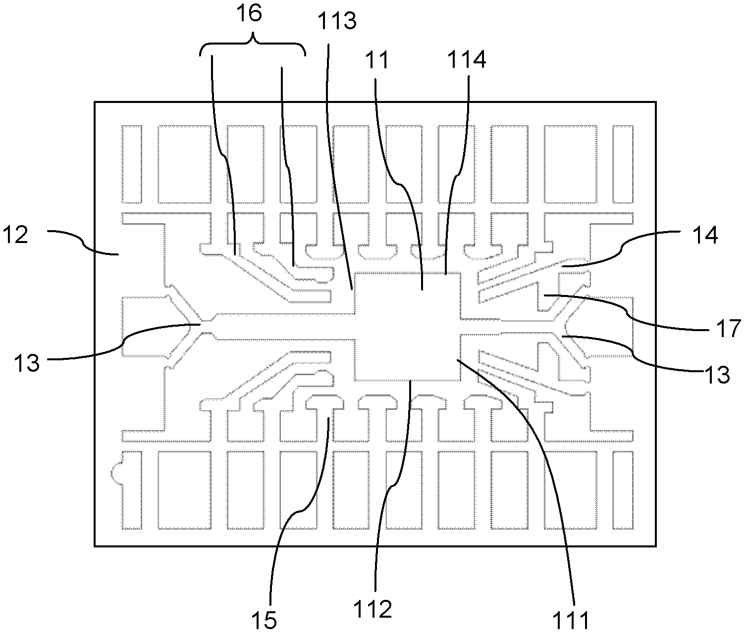
[0017] see figure 1 and combine figure 2 As shown, the lead frame 1 is formed by stamping flat metal, which includes a square wafer carrier 11 i...


PUM


Abstract

The invention provides a semiconductor chip which comprises a lead frame, a wafer provided at one side of the lead frame, a routing connecting with the wafer and the lead frame, and a packaging housing which covers the wafer, the lead frame and the routing. The lead frame comprises a supporting part for placing the wafer at a center and a pin which is connected with the wafer through the routing. The semiconductor chip also comprises a crystal oscillator which is provided at the other side of the lead frame and is opposite to the wafer. Extending from the pin of the lead frame, a welding joint is formed. The pin of the crystal oscillator is welded to the welding joint. The crystal oscillator and the wafer of the semiconductor chip are packaged together, an integrated level is high, and working stability of the chip is high.

Description

【Technical field】 [0001] The invention relates to a semiconductor chip, in particular to the improvement of the internal packaging structure of the semiconductor chip. 【Background technique】 [0002] A semiconductor chip is usually an integrated circuit composed of many transistors that can perform certain functions. Usually, a chip needs an external clock to provide an accurate clock frequency. In order to ensure the reliable function of the integrated circuit, the clock frequency provided to the circuit must be stable and reliable. Existing chips are generally installed on a circuit board, and the clock frequency is provided by an external crystal oscillator, but such a chip provided by an external crystal oscillator will occupy a certain amount of space, and the area occupied by the entire circuit is relatively large. , the integration level is not high, and secondly, because the crystal and the chip are separated, the working environment will always be different, so that...

Claims


Application Information

Patent Timeline
IPC IPC(8): H01L23/495H03H9/19
CPCH01L2224/48091H01L2224/48247H01L2924/00014
Inventor 顾奇龙薛茗泽
Owner RFDOT MICROELECTRONICS
Learn More