Detection method of scanning electron microscope

A technology of electron microscope and detection method, which is applied in the detection field of scanning electron microscope, can solve the problems such as difficult to meet the requirements of precision, affect the production capacity of the machine, and difficult to meet the requirements of detection speed, so as to achieve the effect of improving work efficiency

Active Publication Date: 2012-05-02
SHANGHAI HUALI MICROELECTRONICS CORP
View PDF8 Cites 35 Cited by
  • Summary
  • Abstract
  • Description
  • Claims
  • Application Information

AI Technical Summary

Problems solved by technology

[0006] When using this existing method for wafer defect detection, since the deviation value is obtained by operating on the wafer-level scan image, what this method corrects is a larger range (wafer-level ) deviation, its accuracy is low, and it is difficult to capture defects through one inspection. Usually, it is necessary to compare images in a relatively large range to determine the exact location of the defect, so as to complete the final inspection. Such inspections will cost more A lot of time will affect the production capacity of the machine
[0007] With the development of integrated circuit technology, the size of the chip is getting smaller and smaller, and the size of the defect on the wafer is also getting smaller and smaller, which will bring more and more problems to confirm its shape with a scanning electron microscope. Difficulty, the existing above-mentioned detection methods have actually been difficult to meet the accuracy requirements of actual production
Since the number of defects on a wafer is related to its production quality, the detection and observation of defects has become very important. In addition, the size of the wafer will become larger and larger, and the number of defects that need to be inspected on the wafer will increase. , the existing detection methods are still difficult to meet the detection speed requirements of actual production

Method used


Image

  • Detection method of scanning electron microscope
  • Detection method of scanning electron microscope
  • Detection method of scanning electron microscope

Examples


Embodiment 1

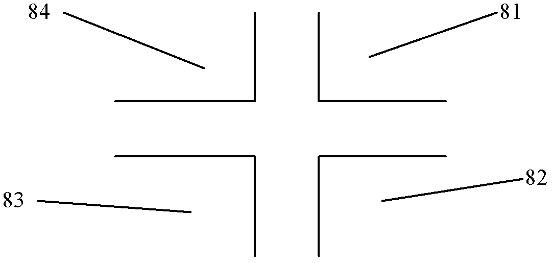
[0041] Please refer to figure 2 and also refer to Figure 7 . figure 2 is a schematic diagram of the definition of the chip corner. exist figure 2 In the figure, a part of four chips such as chip one 81 to chip four 84 and a "cross"-shaped space formed between these four chips are shown. In this embodiment, the geometric center (intersection) of the "cross"-shaped void part is defined as the "chip corner" described in the present invention. In a wafer, a chip corner can be formed between any four adjacent chips. Since the size of a single chip is often very small relative to the size of the wafer, in order to select the convenience and accuracy of the starting position, it is first necessary to select a certain chip corner as the starting position of defect detection.

[0042] However, it should be noted that the "chip corner" may also be selected as a certain corner of a single chip, which is not specifically limited in the present invention.

[0043] Please refer to...

Embodiment 2

[0051] The main parts of this embodiment are the same as those of Embodiment 1, and only the parts different from Embodiment 1 will be described below. After obtaining the chip-level deviation value, use the deviation value and the above-mentioned wafer-level deviation value to correct the coordinates obtained by the defect scanning machine for all defects on chip C4, and perform point-by-point scanning and photographing. Select another chip C5 afterwards, obtain the deviation value (Z5, W5) of the chip level of chip C5 again with the method described in embodiment 1, then obtain the defect scanning machine of all defects on the chip C5 according to the above-mentioned method The obtained coordinates are corrected, scanned point by point and photographed. By analogy, a corresponding chip-level deviation value (Zn, Wn) is obtained for each chip Cn, and this deviation value is used together with the wafer-level deviation value to correct defects in the chip, and the above method...

Embodiment 3

[0053] Different from Embodiment 2, in order to improve the detection efficiency, after obtaining the deviation value of the wafer level and the deviation value of the chip level of a selected chip, all defects on the wafer to be tested can be obtained in the defect scanning machine. The coordinates are corrected, and the image is captured.


PUM


Abstract

The invention relates to a detection method of a scanning electron microscope. The detection method can be used for detecting the defect of a wafer provided with a plurality of chips, and comprises the steps of: importing a file of the wafer with a defect; putting the wafer to be detected on an objective table of the scanning electron microscope; setting a corner of a certain chip arranged on the wafer to be detected as an initial position; correcting the position of the wafer to be detected; obtaining the offset value of the levels of the wafers arranged at the central parts of cavities of two machine types; selecting the chip to be detected, and correcting the coordinate of the corner of the chip in a defect scanning machine according to the offset value of the levels of the wafers; leading the corner of the chip to be moved to the center of the image of a display device in a state of amplifying the image, and obtaining the offset value of the levels of the chips arranged at the central parts of the cavities of the two machine types; obtaining the corrected coordinate of the defect based on the offset value of the levels of the wafers and the offset value of the levels of the chips; and according to the corrected coordinate of the defect, leading the defect to be detected to be positioned under an electron gun of the defect scanning machine, and therefore, the feature of the defect can be rapidly and accurately caught.

Description

technical field [0001] The invention relates to a scanning electron microscope detection method, in particular to a scanning electron microscope detection method for quickly detecting wafers. Background technique [0002] In the manufacturing process of semiconductor devices, the detection of wafers is very important to ensure the quality of products. By detecting and analyzing the defects of the wafer, the cause of the defects can be found, thereby improving the yield and stabilizing the operation of the production line. [0003] Currently, inspection of wafers for defects using a scanning electron microscope is a relatively common method. The basic structure of the scanning electron microscope in the prior art will be briefly described below. [0004] see figure 1 , figure 1 It is a schematic diagram of the main structure of the existing scanning electron microscope. Such as figure 1 As shown, the scanning electron microscope mainly includes a display, a lens barrel ...

Claims


Application Information

Patent Timeline
Patent Type & Authority Applications(China)
IPC IPC(8): G01N23/22
Inventor 倪棋梁陈宏璘龙吟郭明升
Owner SHANGHAI HUALI MICROELECTRONICS CORP
Why Eureka
Try Eureka