Touch panel
A touch panel and substrate technology, applied in the direction of instruments, electrical digital data processing, input/output process of data processing, etc., can solve the problems of complicated assembly procedures, excessive production materials, waste of man-hours, etc., and achieve adhesion and reliability The effect of increased etchability
- Summary
- Abstract
- Description
- Claims
- Application Information
AI Technical Summary
Problems solved by technology
Method used
Image
Examples
Embodiment Construction
[0029] Embodiments of the touch panel according to the present invention will be described below with reference to related drawings. For ease of understanding, the same components in the following embodiments are marked with the same symbols for illustration.
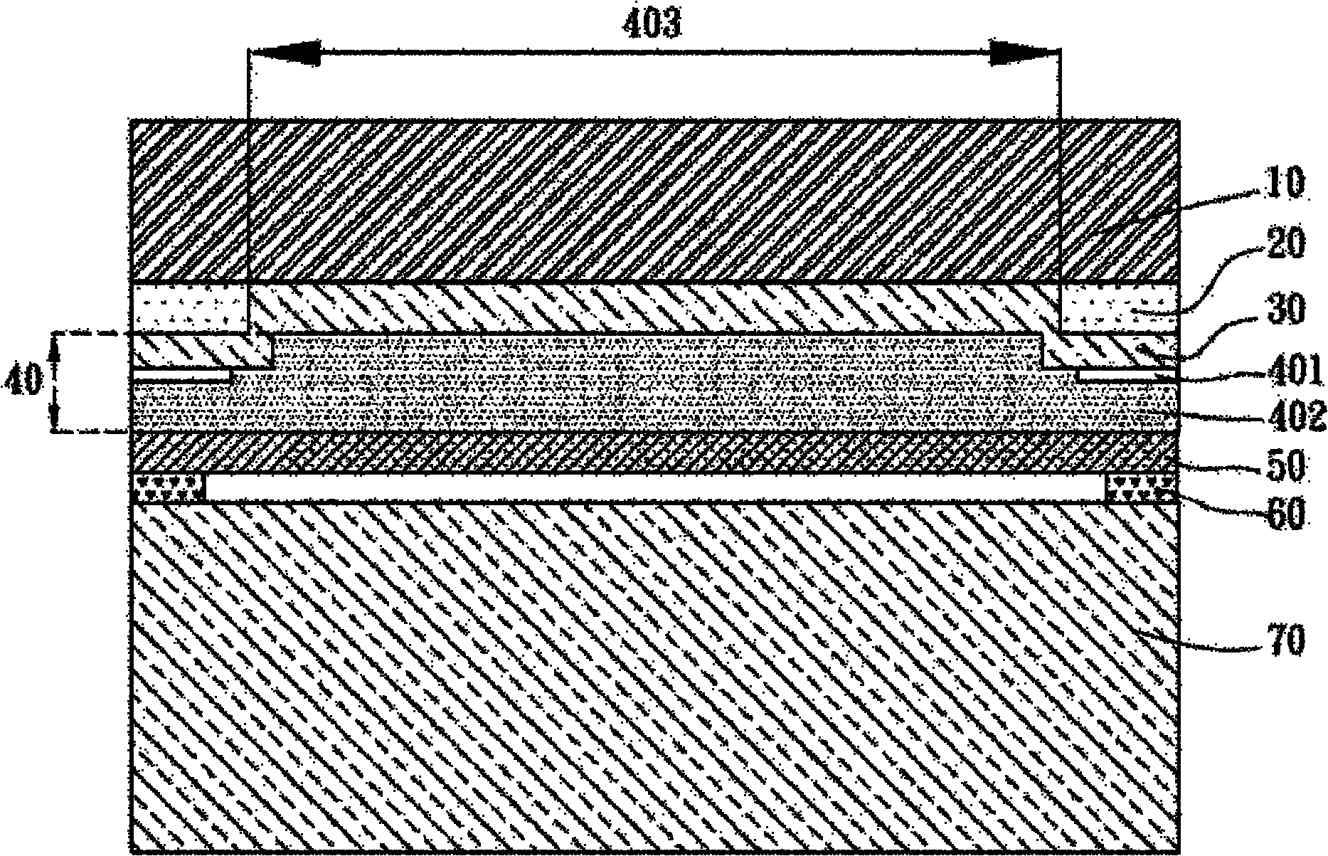
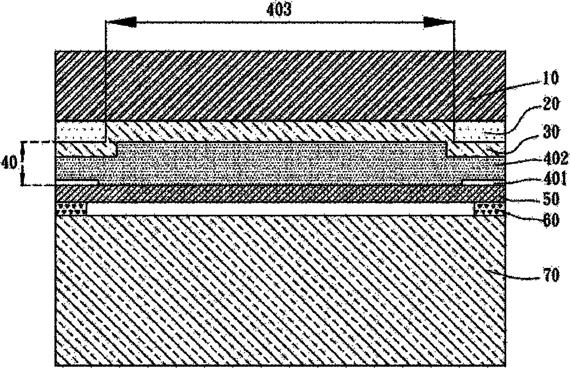
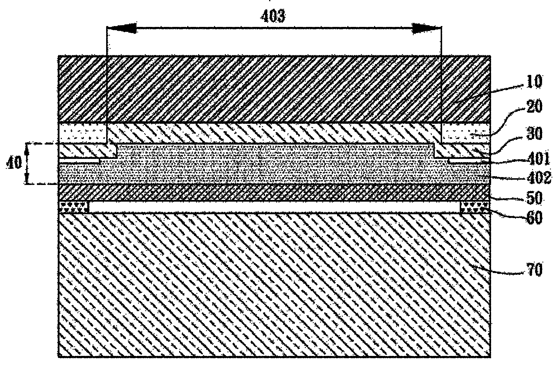
[0030] see figure 1 , which is a cross-sectional view of the first embodiment of the touch panel of the present invention. Such as figure 1 As shown, the touch panel includes: a substrate 10, a shielding layer 20, a sensing circuit layer 40 and an isolation layer 30. The substrate 10 can be glass, for example, which has a top surface and a bottom surface respectively. The shielding layer 20 Formed on the periphery of the bottom surface of the substrate 10, it is a "black matrix" (Black Matrix) or other coating with a shielding effect, which can be a metal layer or an organic layer. In addition, the sensing circuit layer 40 is arranged on the substrate 10 and is connected with the shielding layer 20 Located on the same...
PUM
 Abstract
Description
Claims
Application Information


