Method for producing crystalline-state high-K gate dielectric material

A technology of dielectric materials and gate dielectrics, applied in the application of crystalline high-K gate dielectric materials in MOSFET devices, and in the field of crystalline high-K gate dielectric materials used to form Ge-based MOSFET devices, which can solve interface state problems, etc. problem, to achieve the effect of solving the interface state problem

Inactive Publication Date: 2012-05-02
INST OF MICROELECTRONICS CHINESE ACAD OF SCI
View PDF3 Cites 6 Cited by
  • Summary
  • Abstract
  • Description
  • Claims
  • Application Information

AI Technical Summary

Problems solved by technology

[0006] In view of this, the main purpose of the present invention is to provide a method for making crystalline high-K gate dielectric materials, to solve the interface state problem of Ge-based MOS field effect transistors, and to obtain high-performance Ge-based MOS devices

Method used


Image

  • Method for producing crystalline-state high-K gate dielectric material
  • Method for producing crystalline-state high-K gate dielectric material
  • Method for producing crystalline-state high-K gate dielectric material

Examples


Embodiment Construction

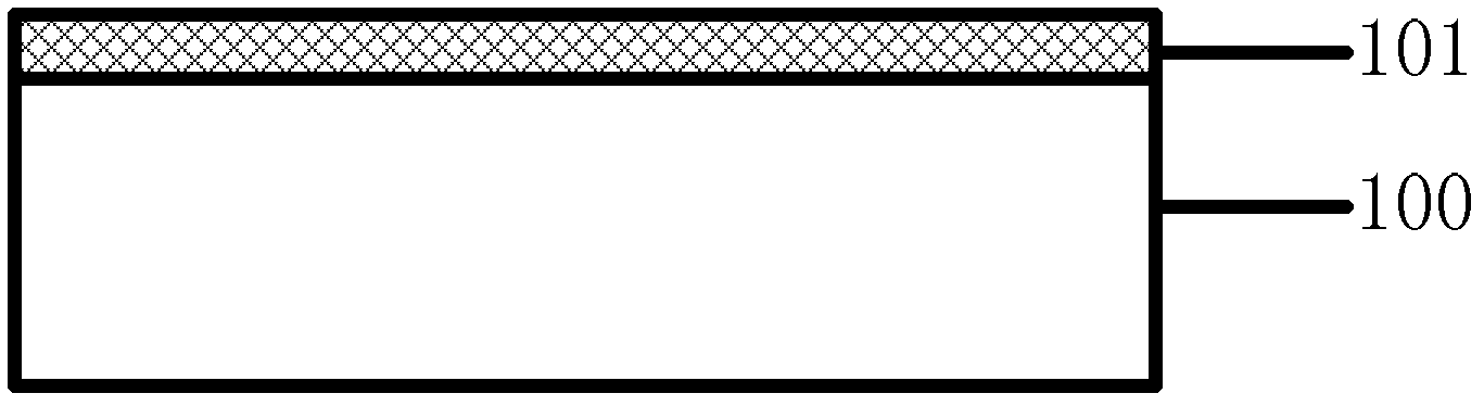
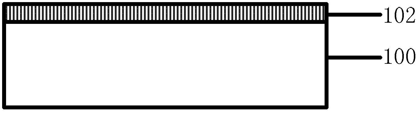
[0023] In order to make the object, technical solution and advantages of the present invention clearer, the present invention will be described in further detail below in conjunction with specific embodiments and with reference to the accompanying drawings. For the convenience of illustration, the thicknesses of layers and regions are enlarged or reduced, and the sizes shown do not represent actual sizes, but only reflect the mutual positions between regions and constituent structures, especially the up-down relationship between structures.

[0024] The method for producing a crystalline high-K gate dielectric material provided by the present invention comprises depositing an amorphous high-K gate dielectric material on a single crystal substrate, and crystallizing the amorphous high-K gate dielectric material into a crystalline state by means of an annealing process. State high-K gate dielectric material; or direct epitaxial growth of crystalline high-K gate dielectric materia...


PUM

PropertyMeasurementUnit
thicknessaaaaaaaaaa

Abstract

The invention discloses a method for producing a crystalline-state high-K gate dielectric material, which comprises the following steps that: an amorphous high-K gate dielectric material is deposited on a single-crystal underlay, and the amorphous high-K gate dielectric material is crystallized to the crystalline-state high-K gate dielectric material through an annealing process; or the crystalline-state high-K gate dielectric material is directly epitaxially grown on a germanium (Ge) underlay. Due to the adoption of the method for producing the crystalline-state high-K gate dielectric material provided by the invention, crystallographic lattice constant of the crystalline-state high-K gate dielectric material grown on Ge is approximate to that of the Ge, an interface structure with low-flaw density can be formed, so the interface state problem of a Ge-based metal oxide silicon (MOS) field effect transistor can be solved, and a Ge-based MOS part with high performance can be further obtained.

Description

technical field [0001] The invention relates to the technical field of semiconductor integrated circuits, in particular to a method for manufacturing a crystalline high-K gate dielectric material used to form Ge-based MOSFET devices, and the application of the crystalline high-K gate dielectric material to MOSFET devices. Background technique [0002] With the continuous shrinking of silicon (Si)-based metal oxide semiconductor field effect transistor (MOSFET) feature size, the performance of traditional planar Si-based devices has reached the end of technology, which requires further research on substrate materials and device structures. Innovate to further improve device performance. Compared with Si, germanium (Ge) has many advantages, among which the carrier mobility is very high (electron mobility is 2 times that of Si, hole mobility is 4 times that of Si, which is the highest among semiconductor materials) , small drive current, and suitable for low-temperature proces...

Claims


Application Information

Patent Timeline
Patent Type & Authority Applications(China)
IPC IPC(8): H01L21/285H01L21/28C23C14/08
Inventor 刘洪刚薛百清常虎东孙兵王盛凯卢力王虹
Owner INST OF MICROELECTRONICS CHINESE ACAD OF SCI
Why Eureka
Try Eureka