Semiconductor light-emitting device

A technology for light-emitting devices and semiconductors, applied in semiconductor devices, electrical components, circuits, etc., can solve problems such as adverse effects, and achieve the effects of improving efficiency, reducing photo-oxidation pressure, and reducing heat generation effects.

Active Publication Date: 2014-12-24
ZHEJIANG SMART LIGHTING TECH
View PDF6 Cites 0 Cited by
  • Summary
  • Abstract
  • Description
  • Claims
  • Application Information

AI Technical Summary

Problems solved by technology

[0007] The purpose of the present invention is to provide a semiconductor light-emitting device, adding an optical filter layer, cutting off a large amount of short-wave blue light, which is beneficial to human health, and solves the problem of short-wave blue light adversely affecting the human body; at the same time, the cut-off short-wave blue light Reflection re-excites the phosphor, improves long-wavelength emission, and improves luminous efficiency

Method used


Image

  • Semiconductor light-emitting device
  • Semiconductor light-emitting device
  • Semiconductor light-emitting device

Examples


Embodiment 1

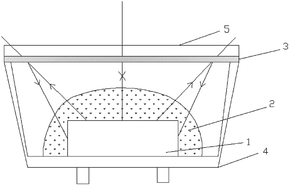
[0033] Example 1: A semiconductor light-emitting device, comprising a base 4, a semiconductor PN junction light-emitting chip 1 arranged on the base 4, a phosphor layer 2 coated on the periphery of the light-emitting chip 1, and a light-transmitting cover arranged on the periphery of the phosphor layer 2 The shell 5, and the optical filter layer 3 surrounding the phosphor layer 2. In a preferred solution, the optical filter layer 3 is disposed on the inner surface of the transparent casing 5 . Such as figure 1 As shown, the light-transmitting cover 5 is made of resin or other light-transmitting materials, which is planar, so the corresponding optical filter layer 3 is also planar.

[0034] Semiconductor PN junction light-emitting chip 1 emits blue light, part of which is absorbed by phosphor layer 2, and phosphor layer 2 emits yellow light with a longer wavelength after being excited by blue light; the other part of blue light is directly mixed with yellow light after passi...

Embodiment 2

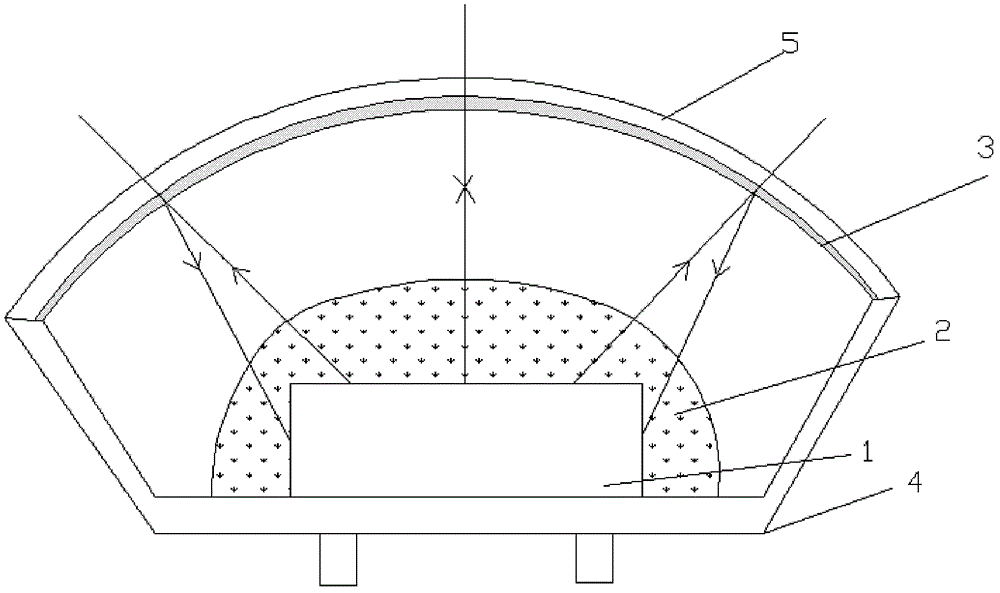
[0037] Example 2: A semiconductor light emitting device, such as figure 2 As shown, the light-transmitting cover 5 is an arc-shaped surface formed centering on the light-emitting chip 1 , among which a concave surface is preferred. Then the optical filter layer 3 matched with the light-transmitting cover 5 is also concave, and the concave optical filter layer 3 can fully reflect the light emitted by part of the light-emitting chip 1 to the phosphor layer 2 to improve the reflection. The utilization efficiency of light improves the photometric and chromaticity performance and luminous efficiency of the phosphor layer 2 . All the other structures are with embodiment 1.

Embodiment 3

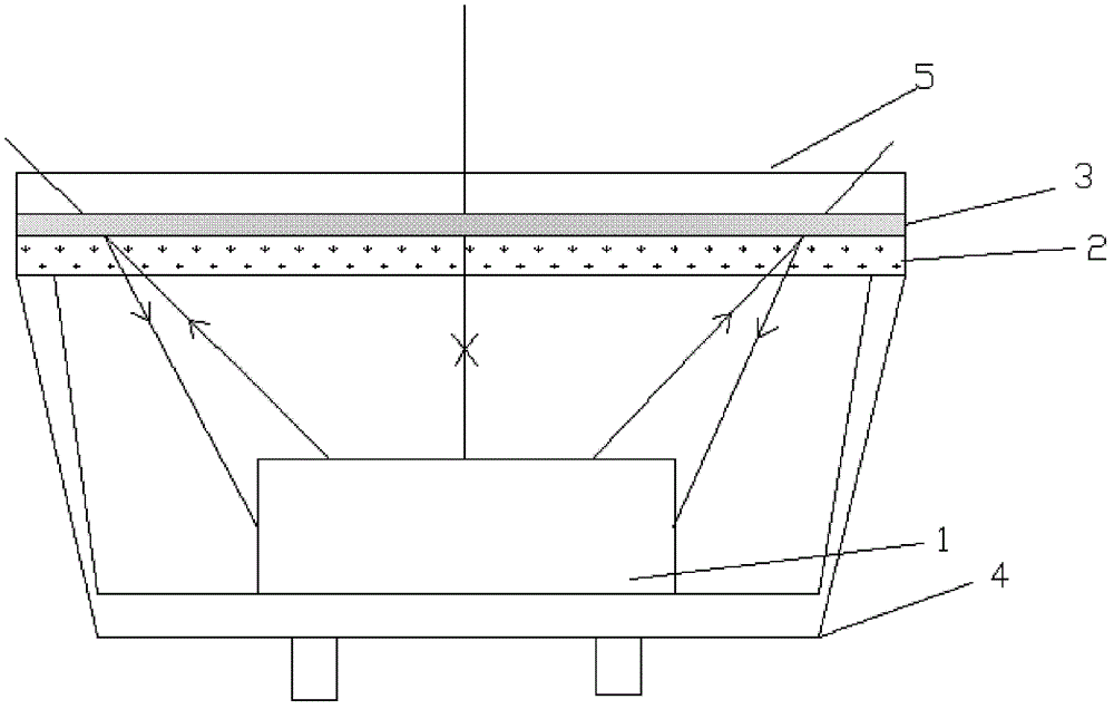
[0038] Example 3: A semiconductor light emitting device, such as image 3 Or as shown in 4, the phosphor layer 2 is made into a film layer, covering the surface of the optical filter layer 3 near the light-emitting chip 1 . The phosphor layer 2 is not directly coated on the light-emitting chip 1, but is directly coated on the inner surface of the optical filter layer 3, and there is a certain gap between the light-emitting chip 1 and the light-emitting chip 1 and the phosphor layer 2. The direct contact is beneficial to the heat dissipation of the light-emitting chip 1 . On the one hand, this method can ensure that the covering thickness of the phosphor layer 2 is consistent, and improves the light color stability; on the other hand, it can reduce the influence of the temperature of the light-emitting chip 1, effectively reduce the junction temperature, improve the luminous efficiency, and have good performance. All the other structures are with embodiment 1 or embodiment 2...


PUM


Abstract

The invention relates to a semiconductor light-emitting device. The semiconductor light-emitting device comprises a base, a semiconductor PN junction light-emitting chip, a fluorescent powder layer and a light transmission housing, wherein the semiconductor PN junction light-emitting chip is disposed on the base; the fluorescent powder layer is cladded at the periphery of the light-emitting chip; and the light transmission housing is covered at the periphery of the fluorescent powder layer. The semiconductor light-emitting device is characterized by further comprising an optical filter layer which is wrapped at the periphery of the fluorescent powder layer. The optical filter layer is a selective projection / reflection filter layer which can reflect short waves and project long waves, namely, the optical filter layer reflects short wavelength lights emitted by the chip and projects long wavelength lights emitted by the fluorescent powder layer. The invention has the prominent substantial characteristics that the optical filter layer is added to cut a part of blue lights, so that light oxidation pressure of blue lights to retina and photochemical injury are reduced, especially the injury to the group with pathological changes of retina is reduced; and light-emitting efficiency is improved. A reflection layer is disposed on the base, and a reflection cavity is formed between the reflection layer and the optical filter layer, so that fluorescent powder is stimulated fully.

Description

technical field [0001] The invention relates to a semiconductor light emitting device. Background technique [0002] LED is a semiconductor light-emitting device that can convert electrical energy into light energy. Compared with incandescent lamps and tungsten halogen lamps for general lighting, LED lighting is favored due to its energy saving, environmental protection, long life, fast response, resistance to switch impact, easy light distribution and many other advantages. TV backlighting gradually enters the field of general lighting. [0003] According to the research on visible light, to obtain white LEDs, at least a mixture of multiple spectra is required, such as white LEDs with two wavelengths (blue light + yellow light) or three wavelengths (blue light + green light + red light). [0004] At present, white light LEDs are mainly made by encapsulating a blue-emitting GaN chip and a phosphor layer coated above it. Under the excitation of short-wave blue light, the p...

Claims


Application Information

Patent Timeline
Patent Type & Authority Patents(China)
IPC IPC(8): H01L33/58H01L33/50
Inventor 王建平牟同升
Owner ZHEJIANG SMART LIGHTING TECH
Why Eureka
Try Eureka