Automatic power control circuit for driving optical communication laser

An automatic power control and laser technology, applied in lasers, laser parts, semiconductor lasers, etc., can solve the problems of complex design and negative feedback loop stability, etc. The effect of occupying a small chip area

Active Publication Date: 2012-05-02
FENGHUO COMM SCI & TECH CO LTD +1
View PDF6 Cites 11 Cited by
  • Summary
  • Abstract
  • Description
  • Claims
  • Application Information

AI Technical Summary

Problems solved by technology

The usual design implementation method is to use an amplifier to form a negative feedback loop to lock the bias voltage at both ends of the photodiode PD so that it is around 2V. The difficulty of doing this lies in the capacitance C MD Outside the chip (outside the LDD chip), it has a greater impact on the stability of this negative feedback loop. At the same time, it is also necessary to consider the impact of this negative feedback loop on the stability of the entire APC control loop. The design is more complicated.

Method used


Image

  • Automatic power control circuit for driving optical communication laser
  • Automatic power control circuit for driving optical communication laser
  • Automatic power control circuit for driving optical communication laser

Examples


Embodiment Construction

[0073] The present invention will be described in further detail below in conjunction with the accompanying drawings.

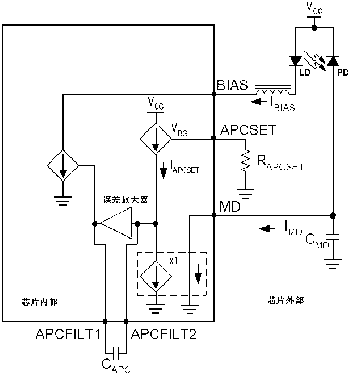
[0074] The automatic power control circuit for optical communication laser driver described in the present invention, such as image 3 shown ( image 3 The part above the dotted horizontal line indicates the external circuit and components of the chip), including: an error amplifier,

[0075] DC reference stable voltage V REF Connected to the positive input terminal VIP of the error amplifier,

[0076] Node APCFILT2 is connected to the negative input terminal VIN of the error amplifier,

[0077] The output VOUT of the error amplifier is connected to node APCFILT1,

[0078] Node APCFILT1 and node APCFILT2 are respectively connected to the capacitor C outside the chip APC both ends of

[0079] Node ACPFILT1 is also connected to the gate of NMOS transistor MN1,

[0080] The drain of transistor MN1 is connected to the power supply V DD , the source is con...


PUM


Abstract

The invention relates to an automatic power control circuit for driving an optical communication laser. The circuit comprises an error amplifier, wherein the VIP end of the error amplifier is connected with a direct current reference stabilized voltage VREF, and the VIN end of the error amplifier is connected with a node APCFILT2; the VOUT end of the error amplifier is connected to a node APCFILT1; a transistor MN1 and a current source I1 form a source follower; a direct current reference stabilized voltage VMD_REF is connected to the gate of an N-channel metal oxide semiconductor (NMOS) transistor MN3; the transistor MN3 and a current source I2 form a source follower; transistors MN4 and MN5 form a pair of current mirrors; and transistors MP3 and MP2 form a pair of current mirrors. By the automatic power control circuit for the driving of the optical communication laser, the influence of other poles in the circuit on circuit stability is effectively eliminated, stable direct current voltage offset is provided for a photo diode at the same time, the working performance of the photo diode is improved, a circuit structure is simple and a small chip area is occupied.

Description

technical field [0001] The invention relates to an optical communication laser and belongs to the field of optical communication integrated circuit design, in particular to an automatic power control circuit for driving an optical communication laser. [0002] The automatic power control (Automatic Power Control, or APC for short) circuit can be used to generate the bias current of the laser and automatically control the luminous power of the laser. Background technique [0003] In optical communication, optical fiber is the medium used to transmit optical signals, and laser is the component that generates optical signals, which can complete the conversion from electrical signals to optical signals. The work of the laser is controlled by a dedicated laser diode driver (Laser Diode Driver, or LDD for short) chip. [0004] Usually, a laser is packaged with a laser diode (Laser Diode, or LD) for sending data and a photodiode (Photo Diode, or PD) for power monitoring. The lase...

Claims


Application Information

Patent Timeline
Patent Type & Authority Applications(China)
IPC IPC(8): H01S5/042H03F3/45
Inventor 秦大威
Owner FENGHUO COMM SCI & TECH CO LTD
Why Eureka
Try Eureka