Method for reducing memory effect of chemical mechanical grinding equipment of fixed abrasive particles

A chemical-mechanical and memory-effect technology, used in grinding machine tools, grinding devices, metal processing equipment, etc., can solve the problems of excessive grinding and waste, different number of abrasive particles, insufficient grinding, etc., to save time, improve consistency, Material saving effect

Active Publication Date: 2012-05-16
SEMICON MFG INT (SHANGHAI) CORP +1
View PDF5 Cites 2 Cited by
  • Summary
  • Abstract
  • Description
  • Claims
  • Application Information

AI Technical Summary

Problems solved by technology

However, due to the different factors such as the material of the grinding layer, the height of the grinding step, and the grinding time, the amount of abrasive grains consumed is different.
For example, if the grinding time of the current wafer to be ground is longer or the step height to be ground is higher, more abrasive grains will be consumed. In this case, the grinding pad needs to step forward for a longer distance for the next The wafer to be ground is replenished with more abrasive grains to ensure sufficient grinding of the next wafer to be ground; however, if the grinding time of the current wafer to be ground is short or the step height to be ground is low, the grinding pad will step forward If the length is too large, there will be too much supplementary abrasive grains, which will cause excessive grinding of the next wafer to be ground and lead to waste
[0005] Therefore, it is necessary to improve the memory effect of the existing fixed abrasive chemical mechanical polishing equipment, and set different step lengths for the polishing pad according to the grinding characteristics of the previous wafer, so as to avoid the impact on the next wafer due to insufficient abrasive grains. Insufficient grinding or excessive grinding and waste due to excessive abrasive grains, thereby reducing the memory effect of chemical mechanical grinding with fixed abrasive grains (that is, the grinding of the ground wafer has an impact on the grinding of the next wafer to be ground), and improving Wafer-to-wafer consistency of grinding rate and wafer thickness, improving grinding quality and wafer quality, improving the use value of fixed abrasive chemical mechanical polishing equipment and the reliability of semiconductor devices

Method used


Image

  • Method for reducing memory effect of chemical mechanical grinding equipment of fixed abrasive particles
  • Method for reducing memory effect of chemical mechanical grinding equipment of fixed abrasive particles
  • Method for reducing memory effect of chemical mechanical grinding equipment of fixed abrasive particles

Examples


Embodiment Construction

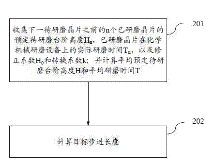
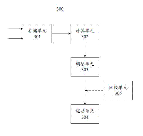
[0053] In the following description, numerous specific details are given in order to provide a more thorough understanding of the present invention. It will be apparent, however, to one skilled in the art that the present invention may be practiced without one or more of these details. In other examples, some technical features known in the art are not described in order to avoid confusion with the present invention.

[0054] In order to provide a thorough understanding of the present invention, in the following description, detailed steps, systems and apparatuses are set forth in order to illustrate the method, system and apparatus of the present invention for reducing the memory effect of fixed abrasive chemical mechanical polishing equipment. Obviously, the practice of the invention is not limited to specific details familiar to those skilled in the semiconductor arts. Preferred embodiments of the present invention are described in detail below, however, the present invent...


PUM


Abstract

The invention relates to a method for reducing the memory effect of chemical mechanical grinding equipment of fixed abrasive particles. The method comprises the following steps of: a) collecting the preset to-be-ground step height Hn of n ground wafers before the next to-be-ground wafer, the actual grinding time Tn, a correction coefficient H0 and a conversion coefficient k; and calculating the average preset to-be-ground step height H and average grinding time T of the ground wafers respectively; and b) calculating a target stepping length IR of the next to-be-ground wafer by a grinding pad according to the following calculation model: IR=k.T(H0+H)/103. The method provided by the invention avoids the conditions of insufficient grinding of the next to-be-ground wafer due to the insufficient abrasive particles on the grinding pad or excessive grinding and waste caused by excessive abrasive particles, and thus reduces the memory effect of chemical mechanical grinding of the fixed abrasive particles, and improves the grinding rate and consistency of wafers with the wafer thickness.

Description

technical field [0001] The present invention relates to fixed abrasive chemical mechanical polishing (Fixed Abrasive Chemical Mechanical Polishing, FACMP) equipment in the semiconductor manufacturing process, and more particularly, the present invention relates to a method for reducing the memory effect (Memory Effect) of fixed abrasive chemical mechanical polishing equipment. Background technique [0002] In the manufacturing process of integrated circuits, various layer structures such as semiconductor layers, conductive layers, and oxide layers are usually deposited sequentially on a silicon wafer. After each layer is deposited, an etching process may be required to form the desired pattern to form the circuit elements. The etching process can lead to uneven or non-uniform surfaces of the deposited layers, which can create defects during subsequent process steps. Therefore, it is necessary to planarize the surface of the device. [0003] Chemical mechanical polishing is...

Claims


Application Information

Patent Timeline
Patent Type & Authority Applications(China)
IPC IPC(8): B24B37/04H01L21/02H01L21/00
Inventor 陈枫
Owner SEMICON MFG INT (SHANGHAI) CORP
Why Eureka
Try Eureka