Compound semiconductor, method for manufacturing the same, semiconductor device, and method for manufacturing the same

Inactive Publication Date: 2005-04-14
PANASONIC CORP
View PDF3 Cites 5 Cited by
  • Summary
  • Abstract
  • Description
  • Claims
  • Application Information

AI Technical Summary

Benefits of technology

[0014] In view of the above-mentioned conventional disadvantages, the present invention has been devised for the purpose of preventing the memory effect produced whe

Problems solved by technology

If the compound semiconductor consisting of the V group element and containing As is dop

Method used


Image

  • Compound semiconductor, method for manufacturing the same, semiconductor device, and method for manufacturing the same
  • Compound semiconductor, method for manufacturing the same, semiconductor device, and method for manufacturing the same
  • Compound semiconductor, method for manufacturing the same, semiconductor device, and method for manufacturing the same

Examples


embodiment 1

[0058] A first embodiment of the present invention will be described with reference to the drawings.

[0059] In the specification of the present application, AlGaInP signifies a compound that contains at least one of aluminum (Al), gallium (Ga), and indium (In) in a III group element, and contains phosphorus (P) in a V group element, and that is expressed by a general formula of AlxGayIn1-x-yP (where x and y satisfy 0≦x≦1, 0≦y≦1, and 0≦x+y≦1). In addition, AlGaAs signifies a compound that contains at least one of aluminum (Al) and gallium (Ga) in a III group element, and contains arsenic (As) in a V group element, and that is expressed by a general formula of AlzGa1-zAs (where z satisfies 0≦z≦1).

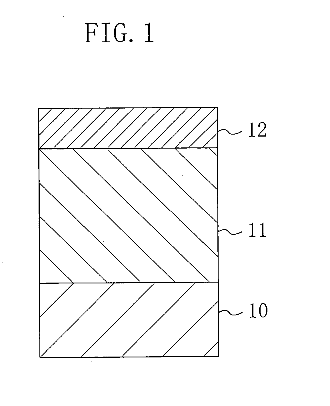
[0060]FIG. 1 shows a sectional configuration of a compound semiconductor (e.g., an epitaxial substrate) in the first embodiment of the present invention. As shown in FIG. 1, the compound semiconductor in the first embodiment is constituted so that a first semiconductor layer 11 that consists...

modification 1

of Embodiment 1

[0066] A compound semiconductor in a first modification of the first embodiment of the present invention will be described with reference to FIG. 3.

[0067]FIG. 3 is a sectional block diagram of the compound semiconductor in the first modification of the first embodiment of the present invention. As shown in FIG. 3, a first semiconductor layer 11 that consists of Al0.35Ga0.15In0.5P and that has a thickness of about 0.5 μm, a second semiconductor layer 22 that consists of Al0.35Ga0.15In0.5P and that has a thickness of about 0.1 μm, and a third semiconductor layer 23 that consists of GaAs and that has a thickness of about 0.3 μm are formed on a substrate 10 consisting of GaAs by epitaxial growth in this order.

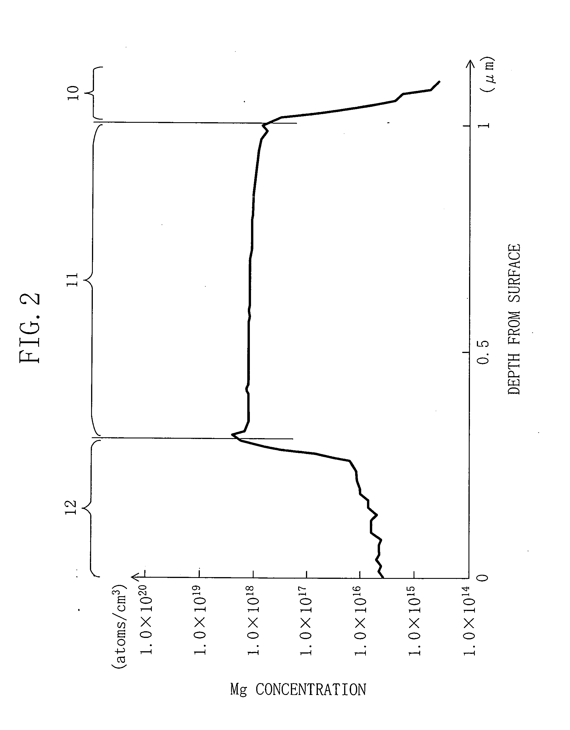
[0068]FIG. 4 is a graph that depicts a result of measuring an Mg concentration profile of the compound semiconductor in the first modification of the first embodiment of the present invention by the SIMS. As can be understood from FIG. 4, the Mg concentration of th...

modification 2

of Embodiment 1

[0075] A second modification of the first embodiment of the present invention will be described with reference to FIGS. 5A and 5B.

[0076] First, as shown in FIG. 5A, a first semiconductor layer 11A that consists of Al0.5Ga0.5As and that has a thickness of about 1 μm and a second semiconductor layer 22 that consists of Al0.35Ga0.15In0.5P and that has a thickness of about 0.2 μm are formed on a substrate 10 consisting of GaAs by the MOCVD method in this order.

[0077] In this second modification, when the first semiconductor layer 11A is to be grown, the layer 11A is grown while adding Mg serving as a p-type dopant thereto so that an Mg concentration is 1×1018 cm−3.

[0078] Next, as shown in FIG. 5B, the second semiconductor layer 22 is removed, for example, by wet etching using an etchant that mainly contains hydrochloric acid (HCl).

[0079] As a result, a compound semiconductor that consists of Al0.5Ga0.5As doped with Mg, that is, a compound semiconductor that does not c...


PUM


Abstract

A first semiconductor layer consisting of AlGaInP is formed on a substrate consisting of GaAs by crystal growth while adding magnesium (Mg) that is a p-type dopant to the first semiconductor layer. A second semiconductor layer consisting of GaAs is then grown on the first semiconductor layer without adding any magnesium to the second semiconductor layer. Thus, the second semiconductor layer can prevent unintended doping (memory effect) produced by magnesium.

Description

CROSS-REFERENCE [0001] All the matters disclosed in claims, specification, and drawings of Japanese Patent Application No. 2003-352035 filed on Oct. 10, 2003 are incorporated herein as reference. BACKGROUND OF THE INVENTION [0002] The present invention relates to a compound semiconductor constituted using a AlGaInP-based semiconductor material, a method for manufacturing the same, a semiconductor device, and a method for manufacturing the same. [0003] A digital versatile disk (DVD) apparatus, which can record information with quite a high density, is rapidly spreading in fields of personal computers and audio-video apparatuses. Recently, a DVD apparatus that can write or re-write information in a DVD is in particular expected to further spread as a next-generation video recorder (DVD recorder) to replace, for example, a mass-storage external memory (e.g., a DVD-R or a DVD-RAM) or a videotape recorder. To this end, it is an important challenge to improve a write rate. [0004] In the D...

Claims


Application Information

Patent Timeline
IPC IPC(8): H01S5/30H01S5/343
CPCB82Y20/00H01S5/34326H01S5/3063H01S5/305
Inventor ONISHI, TOSHIKAZUINOUE, KENICHI
Owner PANASONIC CORP
Why Eureka
Try Eureka