Array substrate, manufacture method thereof and liquid crystal panel

A technology of an array substrate and a manufacturing method, which is applied to the field of array substrates with a narrow frame design, can solve the problems of reducing the utilization rate of a liquid crystal display panel, increasing the size of the frame area 320, etc., and achieves the improvement of display quality, competitiveness and utilization. Effect

Active Publication Date: 2012-05-23
BEIHAI HKC OPTOELECTRONICS TECH CO LTD
View PDF7 Cites 16 Cited by
  • Summary
  • Abstract
  • Description
  • Claims
  • Application Information

AI Technical Summary

Problems solved by technology

This results in an increase in the size of the bezel area 320, reducing the utilization of the LCD panel

Method used


Image

  • Array substrate, manufacture method thereof and liquid crystal panel
  • Array substrate, manufacture method thereof and liquid crystal panel
  • Array substrate, manufacture method thereof and liquid crystal panel

Examples


no. 1 example

[0041] refer to Figure 5 , is a schematic top view structure diagram of the array substrate according to the first embodiment of the present invention.

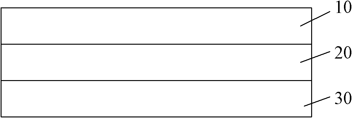
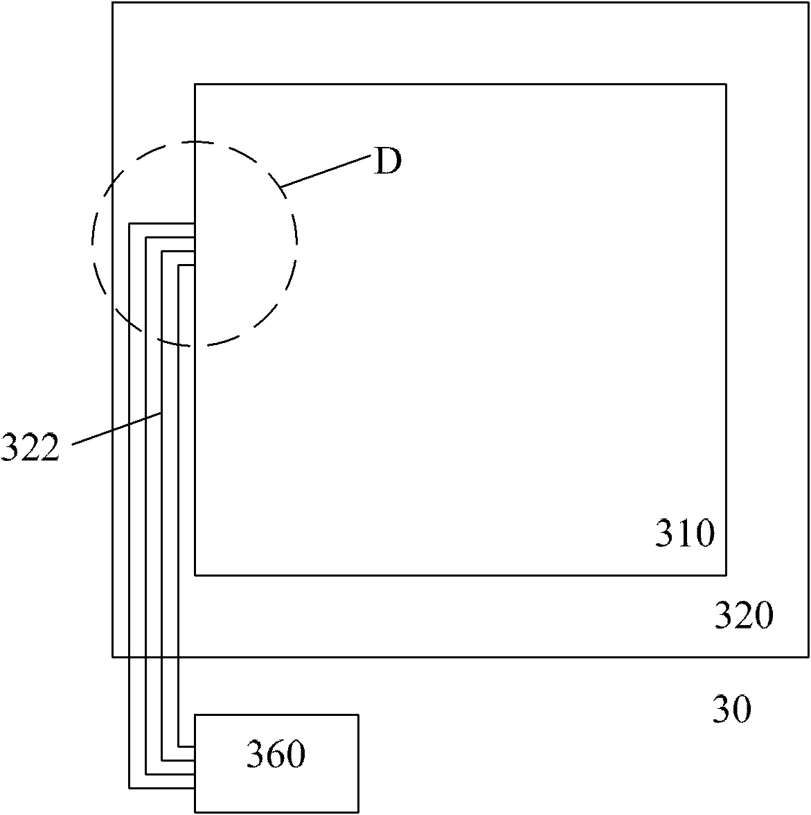
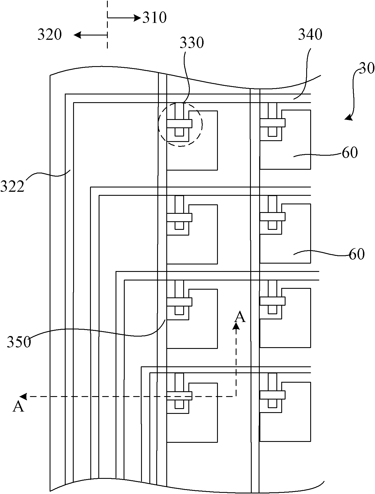
[0042] The array substrate is divided into a display area I and a frame area II surrounding the display area. To simplify the illustration, Figure 52 only shows a schematic top view of the border area of ​​the display area I and the frame area II. The array substrate includes: a glass substrate, multiple scanning lines on the glass substrate: scanning line 101, scanning line 103, scanning line 105, etc., multiple data lines: data line 102, data line 104, data line 106, etc. The scan lines and the data lines are orthogonal and insulated from each other, the data lines are located above the scan lines, and the two divide the display area into a plurality of pixel areas arranged in an array, and each pixel area includes a thin film transistor 110 and pixel electrode 130 .

[0043] Figure 5 The array structure in has 2 row...

no. 2 example

[0054] In the above embodiment, when the scanning connection line and the scanning line extend to the frame area II, they still overlap in the light transmission direction, and a via hole can be directly formed in the frame area II to connect them. Usually, due to the limited width of the scanning connection line and the scanning line, there may be problems of difficult alignment and poor contact when making the via hole, or the problem of disconnection of the scanning line or the scanning connection line. Offset or even failure or disconnection of the line will cause the column of pixel areas controlled by the scan line to fail to work normally. Therefore, the present invention also provides a second embodiment to solve the above problems.

[0055] refer to Figure 6 As shown in FIG. 2 , it is a schematic top view structure diagram of the array substrate according to the second embodiment of the present invention. Will Figure 6 and Figure 5 It can be seen from the compa...


PUM


Abstract

The invention provides an array substrate of a liquid crystal display and a manufacture method of the array substrate, wherein the array substrate is divided into a display region and a frame region which encloses the display region, and the display region is internally provided with a plurality of data lines, a plurality of scanning lines and a plurality of scanning connecting lines; the data lines are intersected with the scanning lines, so that the display region is divided into a plurality of pixel regions; each scanning connecting line and each corresponding scanning line extend to the frame region to be electrically connected with one another, and a driving signal of an external driving chip is transmitted to each scanning line. The scanning lines and the corresponding scanning connecting lines are electrically connected with one another through a plurality of through holes in the frame region, so that the opening rate of the display region can not be influenced, the area of the frame region of the array substrate and the liquid crystal panel can be reduced, and the use ratio of the array substrate and the liquid crystal panel can be improved.

Description

technical field [0001] The invention relates to a liquid crystal panel, in particular to an array substrate with a narrow frame design for reducing the frame width of the liquid crystal display panel and a manufacturing method thereof. Background technique [0002] Flat-panel displays are currently the most popular displays, among which liquid crystal displays are widely used in electronic products such as computer screens, mobile phones, personal digital assistants, and flat-screen TVs because of their thin and light appearance, power saving, and no radiation. [0003] Please refer to figure 1 , for an existing liquid crystal display panel. It includes a color filter substrate 10 and an array substrate 30 opposite to the color filter substrate 10 , and the liquid crystal layer 20 is sandwiched between the color filter substrate 10 and the array substrate 30 . The inner side of the array substrate 30 relative to the color filter substrate 10 is provided with a plurality of...

Claims


Application Information

Patent Timeline
Patent Type & Authority Applications(China)
IPC IPC(8): G02F1/1362G02F1/1333H01L27/12H01L21/77
Inventor 黄贤军赵剑
Owner BEIHAI HKC OPTOELECTRONICS TECH CO LTD
Why Eureka
Try Eureka