Photoresist edge edge-wash data measuring system and measurement monitoring method

A technology of data measurement and photoresist, which is applied in the field of photoresist edge washing data measurement system and measurement monitoring, can solve problems such as unscientific, edge washing line offset cannot be found in time, and performance impact of integrated circuit semiconductor devices. achieve the effect of avoiding the impact

Inactive Publication Date: 2012-05-23
SEMICONDUCTOR MANUFACTURING INTERNATIONAL (BEIJING) CORP +1
View PDF6 Cites 4 Cited by
  • Summary
  • Abstract
  • Description
  • Claims
  • Application Information

AI Technical Summary

Problems solved by technology

Therefore, the offset of the edge washing line cannot be found in time, which will affect the yield rate of integrated circuits and the performance of semiconductor devices
[0007] In order to detect the offset of

Method used


Image

  • Photoresist edge edge-wash data measuring system and measurement monitoring method
  • Photoresist edge edge-wash data measuring system and measurement monitoring method
  • Photoresist edge edge-wash data measuring system and measurement monitoring method

Examples


Embodiment Construction

[0054] The photoresist edge scrubbing data measurement system and measurement monitoring method proposed by the present invention will be further described in detail below in conjunction with the accompanying drawings and specific embodiments. Advantages and features of the present invention will be apparent from the following description and claims. It should be noted that all the drawings are in very simplified form and use imprecise ratios, which are only used for the purpose of conveniently and clearly assisting in describing the embodiments of the present invention.
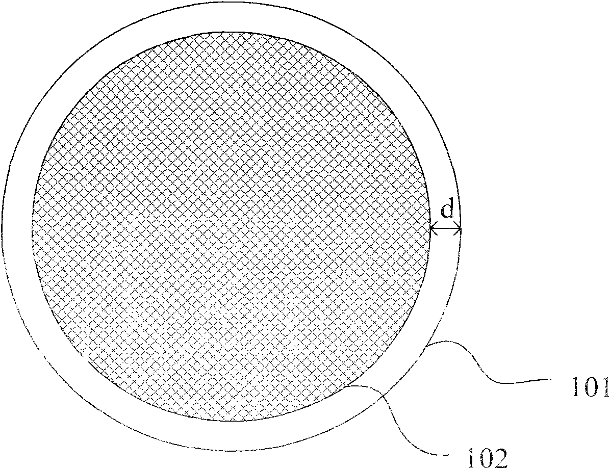
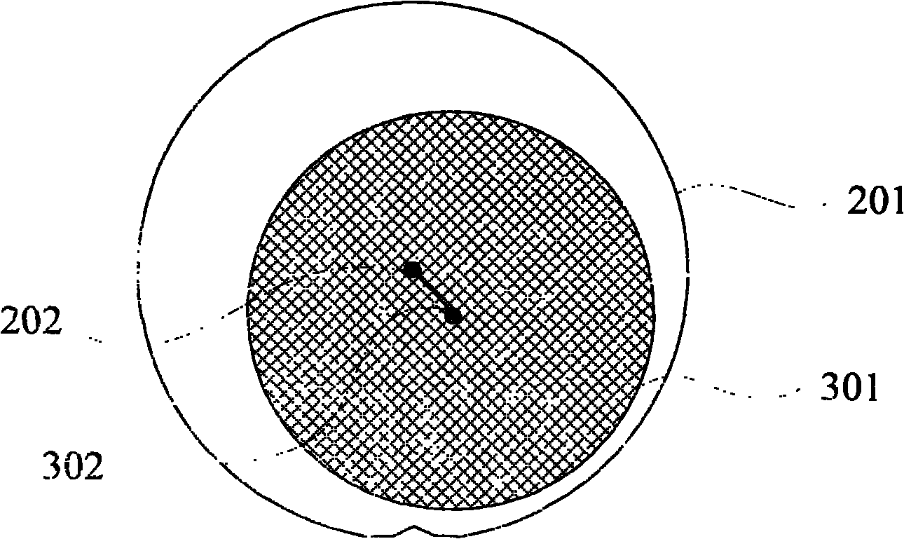
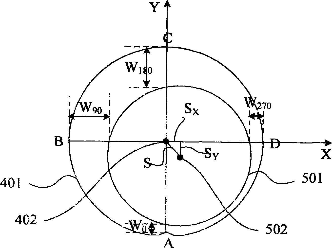
[0055] The core idea of ​​the present invention is to provide a photoresist edge washing data measurement system, the measurement system includes a post-development detection machine, a wafer edge position sensor and an edge washing line position sensor set on the post-development detection machine , a logical operation device and an early warning device installed in the post-development detection machine; t...


PUM


Abstract

The invention discloses a photoresist edge edge-wash data measuring system. The system comprises a developing post-measuring machine, a wafer edge position sensor, an edge-wash line position sensor, a logic operation unit and a pre-warning unit. The system can be used for carrying out developing post-measuring on the wafer and simultaneously calculating the edge-wash width of the photoresist edge and the offset of the edge-wash line, thus the photoresist edge edge-wash data can be obtained in time. The invention further discloses a measurement monitoring method of the photoresist edge edge-wash data, comprising the following steps: measuring and calculating the photoresist edge edge-wash data by using the system; automatically collecting the data, and sending the data to an automatic monitoring system of a semiconductor factory; judging whether the edge-wash width exceeds the maximum allowable width and whether the offset of the edge-wash line exceeds the maximum allowable offset, when exceeds, raising an alarm, and sending the edge-wash width and the offset to workers for measurement. According to the method, the real-time monitoring of the photoresist edge edge-wash data can be realized, and the offset of the edge-wash line can be discovered in time.

Description

technical field [0001] The invention relates to the technical field of semiconductor manufacturing, in particular to a photoresist edge washing data measurement system and a measurement monitoring method. Background technique [0002] The photolithography process is one of the most important process steps in semiconductor manufacturing. The main function of photolithography is to copy the pattern on the mask plate to the semiconductor wafer to prepare for the next etching or ion implantation process. In the photolithography process, the gluing process occupies a very important position, because the quality of the gluing directly determines the quality of the alignment in the lithography process. In the process of gluing, the photoresist usually covers the entire semiconductor wafer. In order to prevent pollution to the semiconductor machine and avoid photoresist burrs on the edge of the semiconductor wafer, it is usually necessary to remove the photoresist in the edge area o...

Claims


Application Information

Patent Timeline
IPC IPC(8): G03F7/20
Inventor 丁海涛
Owner SEMICONDUCTOR MANUFACTURING INTERNATIONAL (BEIJING) CORP
Why Eureka
Try Eureka