
Reaction chamber and semiconductor processing equipment

A reaction chamber and chamber technology, applied in the field of microelectronics, can solve problems such as shortening the time of cold pump pumping capacity, affecting process results, and increasing the number of cold pump regenerations, so as to prolong the regeneration cycle of cold pumps and improve the process Stability, the effect of guaranteeing process results

Active Publication Date: 2018-09-18
BEIJING NAURA MICROELECTRONICS EQUIP CO LTD
View PDF4 Cites 0 Cited by
  • Summary
  • Abstract
  • Description
  • Claims
  • Application Information

AI Technical Summary

Problems solved by technology

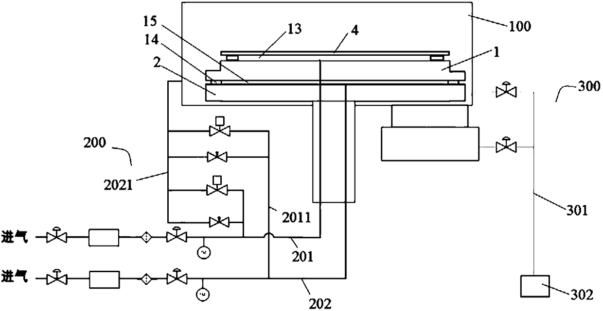
[0006] One, because the lower back-blowing air path 202 needs to supply the back-blowing gas to the back-blowing cavity 15 all the time, and the excess back-blowing gas in the lower back-blowing air path 202 flows into the reaction chamber 100 from the bypass air path, and then It is extracted from the air extraction path, which will affect the pressure rise rate and process pressure of the reaction chamber 100 during the process, thereby affecting the process result;
[0007] Second, due to the limitation of the pumping capacity of the cold pump, it needs to stop the process operation for regeneration when the pumping capacity reaches the set value, and the lower back-blowing air circuit 202 has been supplying the back-blowing cavity 15 to the bottom. Gas reduces the time it takes for the cold pump to reach pumping capacity, causing more cold pump regenerations and impacting capacity

Method used


Image

  • Reaction chamber and semiconductor processing equipment
  • Reaction chamber and semiconductor processing equipment
  • Reaction chamber and semiconductor processing equipment

Examples


Embodiment Construction

[0023] In order to enable those skilled in the art to better understand the technical solution of the present invention, the reaction chamber and semiconductor processing equipment provided by the present invention will be described in detail below with reference to the accompanying drawings.

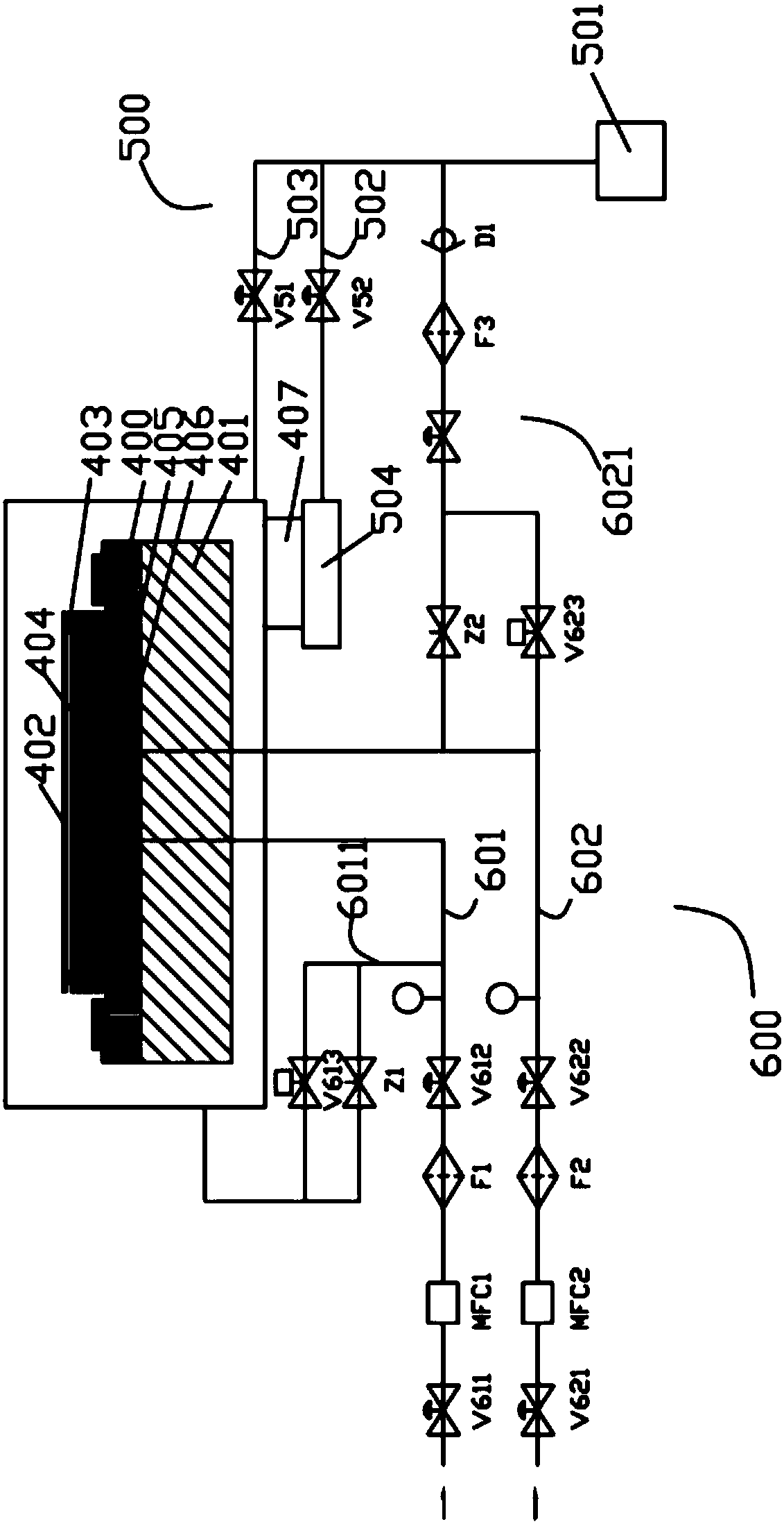
[0024] image 3 A schematic diagram of the gas path of the reaction chamber provided by the embodiment of the present invention. see image 3 , The reaction chamber provided by the embodiment of the present invention includes a chamber pumping system 500 , a wafer holding device and a back blowing gas supply system 600 . Wherein, the chamber pumping system 500 is used to evacuate the reaction chamber, which includes a system dry pump 501, and a first branch 502 and a second branch 503 connected in parallel, and the system dry pump 501 passes through the first branch. The path 503 and the second branch path 502 are connected to the reaction chamber, and are used for initial pumping of ...


PUM


Abstract

The invention discloses a reaction chamber and semiconductor processing equipment. According to the reaction chamber, a back blowing air feeding system comprises an upper back blowing air path and a lower back blowing air path respectively supplying back blowing air for an upper back blowing chamber and a lower back blowing chamber, wherein the upper back blowing air path and the lower back blowing air path respectively have an upper back blowing pumping bypass and a lower back blowing pumping bypass, the upper back blowing pumping bypass is connected with the reaction chamber and is used for transmitting redundant back flowing air of the upper back blowing air path to the reaction chamber, and the lower back blowing pumping bypass is connected with a chamber pumping system and is used for transmitting redundant back flowing air of the lower back blowing air path to the chamber pumping system. The reaction chamber can not only avoid influence of the lower back flowing path on the process, but also can prolong the cold pump regeneration period, and thereby capacity can be improved.

Description

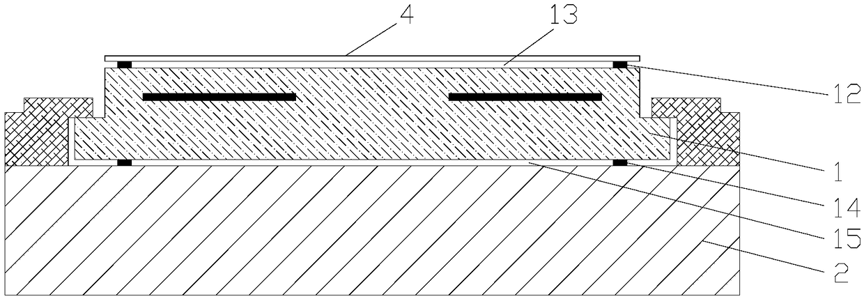
technical field [0001] The invention relates to the technical field of microelectronics, and more specifically, to a reaction chamber and semiconductor processing equipment. Background technique [0002] In the integrated circuit (IC) manufacturing process, especially in the plasma etching (ETCH), physical vapor deposition (PVD), chemical vapor deposition (CVD) and other processes, in order to fix, support and transfer wafers and other processed devices, To avoid movement or dislocation of the processed device, a wafer clamping device such as an Electro Static Chuck (ESC for short) or a mechanical clamp is often used. [0003] At present, a high temperature electrostatic chuck is usually introduced into the manufacturing process of a hard mask (Hardmask) to fix the wafer while controlling the temperature of the wafer. see figure 1 , which shows a common wafer holding device in the prior art. The wafer clamping device includes an electrostatic chuck 1 and a heating base 2 ...

Claims


Application Information

Patent Timeline
Patent Type & Authority Patents(China)
IPC IPC(8): H01L21/67
Inventor 邱国庆
Owner BEIJING NAURA MICROELECTRONICS EQUIP CO LTD
Learn More