Semiconductor device

A technology for semiconductors and devices, applied in the field of semiconductor devices, can solve the problem of expensive backside heat dissipation packaging, and achieve the effects of improving efficiency, shortening distance, and small temperature distribution

Active Publication Date: 2014-12-31
FUJITSU LTD
View PDF6 Cites 0 Cited by
  • Summary
  • Abstract
  • Description
  • Claims
  • Application Information

AI Technical Summary

Problems solved by technology

However, backside-cooled packages are expensive

Method used


Image

  • Semiconductor device
  • Semiconductor device
  • Semiconductor device

Examples


no. 1 example

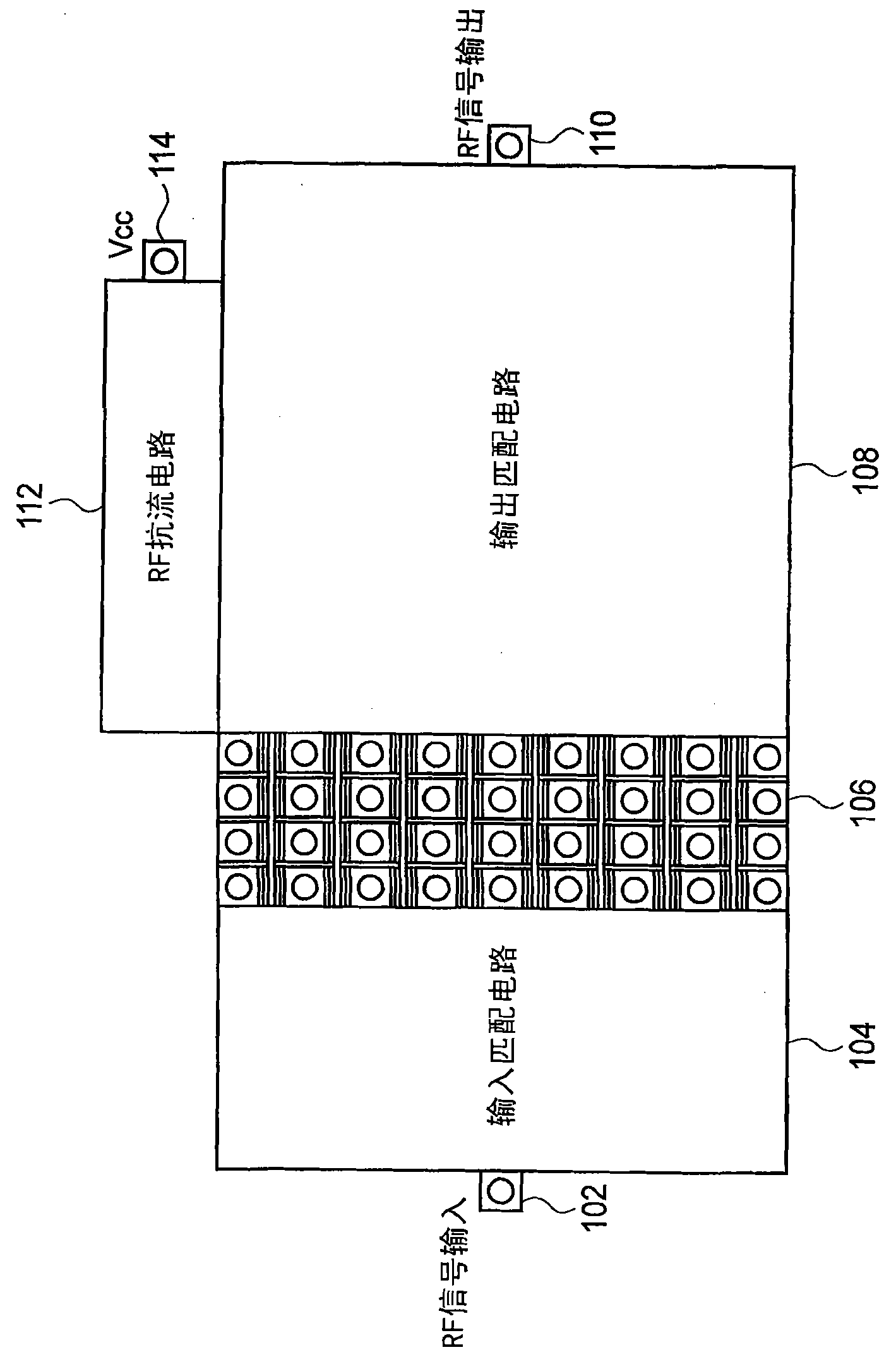
[0026] will refer to Figures 1 to 20C The structure of the semiconductor device according to the first embodiment is described.

[0027] Figure 1 to Figure 4 is a plan view showing the structure of the semiconductor device according to the present embodiment. Figure 5 to Figure 10 is a diagrammatic sectional view showing the structure of the semiconductor device according to the present embodiment. Figure 11A to Figure 12B A sectional view and a plan view showing the structure of a semiconductor device according to a modification of the present embodiment. Figure 13A and Figure 13B is a plan view showing the structure of lead-out lines of the semiconductor device according to the present embodiment. Figure 14 is a schematic cross-sectional view showing a heat dissipation path of the semiconductor device according to the present embodiment. Figure 15 is a graph showing the dependence of the heat dissipation efficiency given by the simulation on the thickness of the ...

no. 2 example

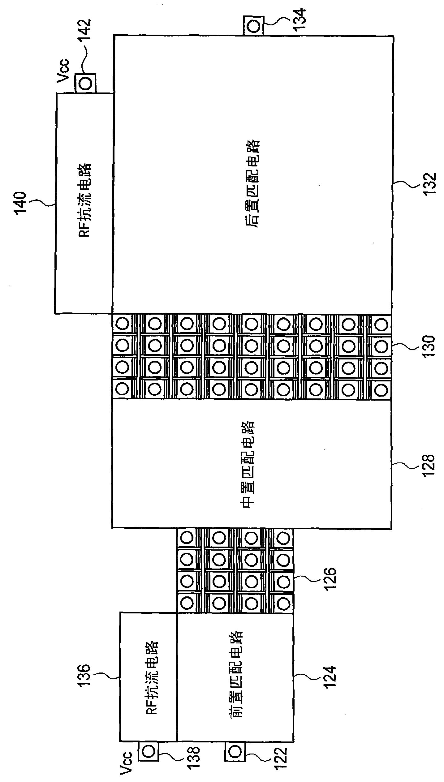
[0081] will refer to Figure 21 to Figure 24 A semiconductor device according to the second embodiment will be described. Elements in this embodiment that are the same as those in the semiconductor device according to the first embodiment are denoted by the same reference numerals to avoid repetition or to simplify description.

[0082] Figure 21 and Figure 22 is a plan view showing the structure of the semiconductor device according to the present embodiment. Figure 23 and Figure 24 is a diagrammatic sectional view showing the structure of the semiconductor device according to the present embodiment.

[0083] The semiconductor device according to the present embodiment is a semiconductor device including high-output transistors, and the semiconductor device according to the present embodiment is the same as that according to the The semiconductor device of one embodiment is the same.

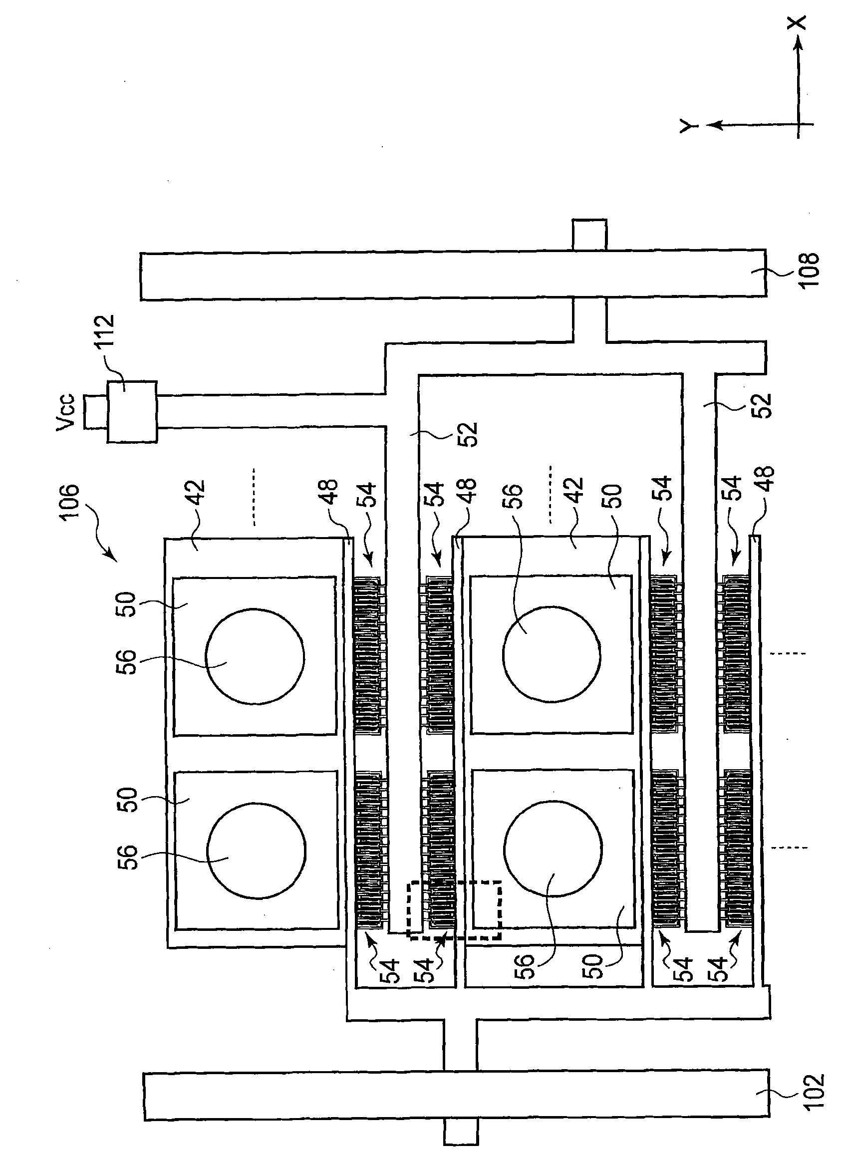
[0084] like Figure 21 As shown, in the transistor integrated unit 106, the pad ...


PUM


Abstract

A semiconductor device includes a transistor array including a plurality of transistors each having a gate electrode extended in a first direction, the plurality of transistors being arranged in a second direction intersecting the first direction, and a pad electrode arranged in the first direction of the transistor array and electrically connected to source regions of the plurality of transistors.

Description

technical field [0001] Embodiments discussed herein relate to a semiconductor device including a power-intensive circuit element. Background technique [0002] A semiconductor device including large power consumption components such as a power amplifier circuit that has a large component heat generation due to operation. In a semiconductor device in which the packing density of circuit elements is increased for high-density mounting, improvement of radio-frequency characteristics, and the like, temperature rise due to operation is more significant. [0003] When the internal temperature of the element exceeds an allowable temperature, circuit characteristics such as high-frequency characteristics degrade, which is a cause of damage to the element in the worst case. Therefore, in a semiconductor device including components with large power consumption, how to radiate heat generated from the components is important. [0004] The following are relevant examples: Japanese Laid...

Claims


Application Information

Patent Timeline
Patent Type & Authority Patents(China)
IPC IPC(8): H01L23/498H01L23/34
CPCH01L2924/0002H01L23/4824H01L27/0207H01L2924/00
Inventor 岛昌司西乡薰三沢信裕佐佐木孝朗
Owner FUJITSU LTD
Why Eureka
Try Eureka