Method for extracting parasitic parameters of interconnection lines and device

A parasitic parameter and interconnection technology, applied in electrical digital data processing, special data processing applications, instruments, etc., can solve the problem of inaccurate extraction results, and achieve the effect of avoiding performance error estimation, accurate parasitic parameters, and consistent performance

Active Publication Date: 2012-06-27
INST OF MICROELECTRONICS CHINESE ACAD OF SCI
View PDF5 Cites 17 Cited by
  • Summary
  • Abstract
  • Description
  • Claims
  • Application Information

AI Technical Summary

Problems solved by technology

The difference in the thickness of the interconnection line will lead to inaccurate extraction results using the parasitic parameter extraction tool of the interconnection line

Method used


Image

  • Method for extracting parasitic parameters of interconnection lines and device
  • Method for extracting parasitic parameters of interconnection lines and device
  • Method for extracting parasitic parameters of interconnection lines and device

Examples


Embodiment Construction

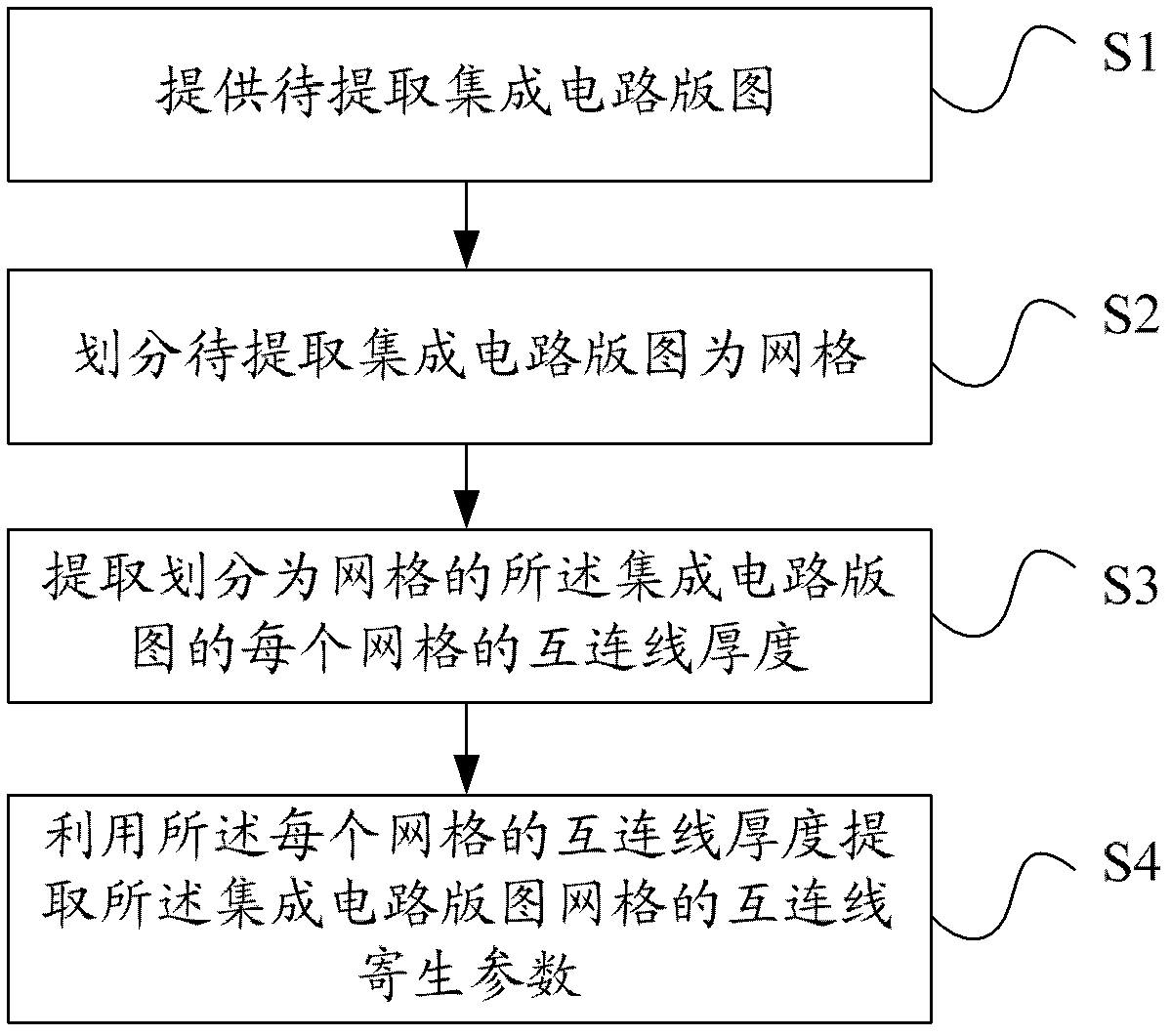
[0021] The following will clearly and completely describe the technical solutions in the embodiments of the present invention with reference to the drawings in the embodiments of the present invention. Apparently, the described embodiments are only some of the embodiments of the present invention, but not all of them. Based on the embodiments of the present invention, all other embodiments obtained by persons of ordinary skill in the art without making creative efforts belong to the protection scope of the present invention.

[0022] Secondly, the present invention is described in detail with reference to the schematic diagrams. When describing the embodiments of the present invention in detail, for the convenience of explanation, the schematic diagrams are only examples, which should not limit the protection scope of the present invention.

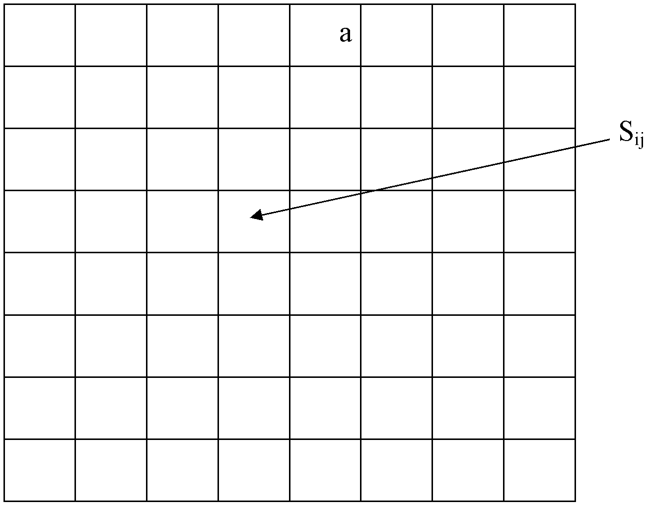
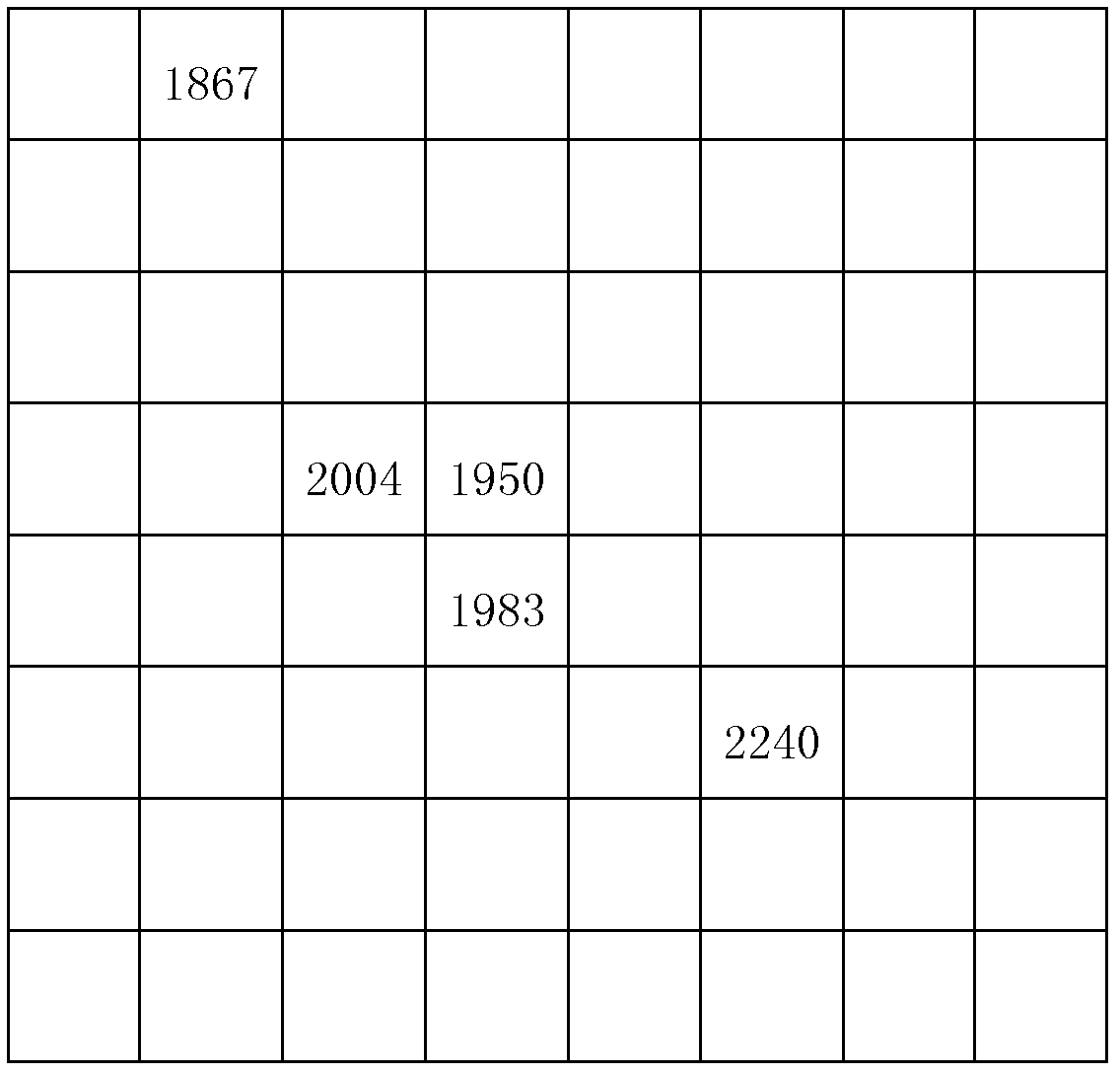
[0023] As mentioned in the background technology, usually when the integrated circuit layout and the deposition process parameters of th...


PUM


Abstract

The invention provides a method for extracting parasitic parameters of interconnection lines. The method includes obtaining the thickness of each interconnection line of each grid of a layout after the integrated circuit layout is divided into the grids in a parasitic parameter extraction process; extracting the parasitic parameters of the interconnection lines of the grids of the layout according to the obtained thicknesses of the interconnection lines so as to obtain parasitic parameter extraction results with consideration of thickness differences. Correspondingly, the invention further provides a device for extracting the parasitic parameters of the interconnection line. The thickness differences of the interconnection lines caused by CMP (chemical mechanical polishing) process are taken into consideration in the method, more accurate geometric information of the interconnection lines is adopted in the parasitic parameter extraction process, and accordingly more accurate parasitic parameters can be obtained.

Description

technical field [0001] The invention relates to the fields of integrated circuit manufacturing and electronic design automation, in particular to a method for extracting parasitic parameters of interconnection lines. Background technique [0002] In the manufacturing process of integrated circuits (Integrated Circuit, IC), metals, dielectrics and other materials are fabricated on the surface of silicon wafers by various methods such as physical vapor deposition and chemical vapor deposition to form electronic components and components. The metal structure layer of the metal interconnection line between each layer is connected with a plurality of metal-filled through holes, which makes the circuit have high complexity and circuit density. An important indicator of integrated circuit performance is path delay, that is, the time required from an input to an output. The path delay of an integrated circuit includes device delay and interconnect delay between devices. With the re...

Claims


Application Information

Patent Timeline
Patent Type & Authority Applications(China)
IPC IPC(8): G06F17/50
Inventor 马天宇陈岚杨飞方晶晶
Owner INST OF MICROELECTRONICS CHINESE ACAD OF SCI
Why Eureka
Try Eureka