Semiconductor equipment
A semiconductor and equipment technology, applied in the field of microelectronics, can solve problems affecting the appearance of the chip and reducing the quality of the chip
- Summary
- Abstract
- Description
- Claims
- Application Information
AI Technical Summary
Problems solved by technology
Method used
Image

Examples
Embodiment Construction
[0037] To enable those skilled in the art to better understand the technical solutions of the present invention, the semiconductor device provided by the present invention will be described in detail below with reference to the accompanying drawings.
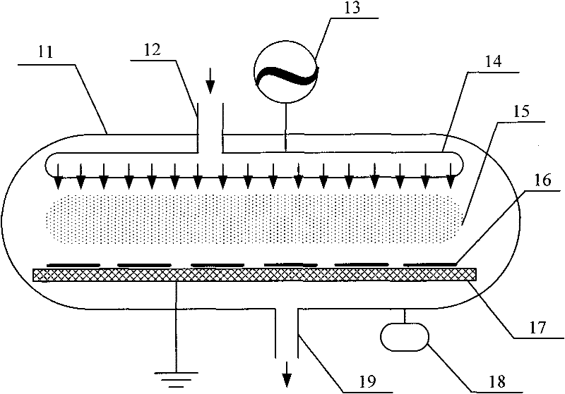
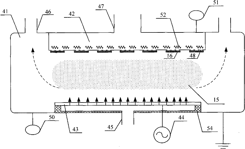
[0038] image 3 It is a schematic diagram of the structure of a semiconductor device provided in the first embodiment of the present invention, such as image 3 As shown, the semiconductor device includes a reaction chamber 41, an adsorption component, and a radio frequency device for providing radio frequency power to the inside of the reaction chamber 41. The adsorption assembly is located inside the reaction chamber 41 and arranged on the top of the reaction chamber 41, and the adsorption assembly is used for adsorbing wafers. An air inlet 45 is provided at the bottom of the reaction chamber 41, and the air inlet 45 is a channel for introducing process gas into the reaction chamber 41.
[0039] In this embodiment, the radio freque...
PUM
 Abstract
Description
Claims
Application Information