Testing device and method for digital semiconductor device

A testing device and semiconductor technology, applied in measurement devices, instruments, measurement electronics, etc., can solve the problems of high cost, small vector storage depth, and low complexity of vector changes, and achieve the effect of reducing testing costs and saving testing time.

Active Publication Date: 2012-07-04
SHANGHAI HUAHONG GRACE SEMICON MFG CORP
View PDF5 Cites 15 Cited by
  • Summary
  • Abstract
  • Description
  • Claims
  • Application Information

AI Technical Summary

Problems solved by technology

The advantage of this memory tester is that it has a large number of digital channels and a large number of simultaneous measurements. The disadvantage is that the vector generator is in ALPG mode, and the generated vector has low complexity and small vector storage depth.
[0003] From this point of view, the two testers have their own characteristics. At present, there are testers that can

Method used


Image

  • Testing device and method for digital semiconductor device
  • Testing device and method for digital semiconductor device
  • Testing device and method for digital semiconductor device

Examples


Embodiment Construction

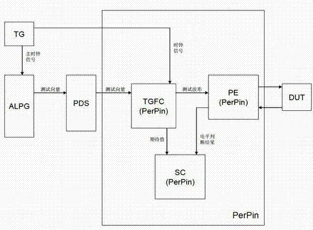
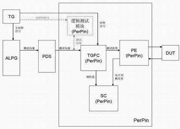
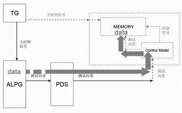
[0023] The invention discloses a test device for digital semiconductor devices, such as figure 2 shown, including:

[0024] A timing generator module that generates a master clock signal;

[0025] The algorithm vector generator module is used to store the test vector information. When the waveform needs to be output to the device under test, the algorithm vector generator module will output the first test vector to the programmable data selector according to the main clock signal sent by the timing generator module In the module, the first test vector is transmitted to each test module resource by switching the PDS internal switch;

[0026] The programmable data selector module receives the first test vector output by the algorithm vector generator module, and transmits the first test vector to the test module resource by switching the internal switch;

[0027] The test module includes a logic test module, a waveform format controller module, a pin circuit module and a digi...


PUM


Abstract

The invention discloses a testing device and method for a digital semiconductor device; the testing device comprises a time series generator module, an algorithm vector generator module, a programmable data selector module and a testing module, wherein the testing module comprises a logic testing module, a waveform format controller module, a base pin circuit module and a digital comparing module; the logic testing module receives a main clock signal and a first testing vector and simultaneously sends a second testing vector to the waveform format controller module; the first testing vector is transmitted to the logic testing module and is stored before testing begins; and when testing begins, the logic testing module selects the stored first testing vector, forms and transmits the second testing vector to the waveform format controller module. The testing device intensifies the functions of a tester of the traditional memory so that the tester not only has the powerful testing function of the traditional memory, but also has the testing capability of a complex logic device; and simultaneously the very strong simultaneous testing capability of the tester is beyond that of the traditional logic tester, thereby effectively reducing the testing cost and saving the testing time.

Description

technical field [0001] The invention relates to a test device, in particular to a test device for digital semiconductor devices. The invention also relates to a testing method, especially a testing method for digital semiconductor devices. Background technique [0002] The advantage of the logic tester is that the digital channels are flexible and changeable. The vector generator is in SQPG mode. The generated vectors have high complexity and large vector storage depth. The tester structure is as figure 1 As shown, it mainly consists of pin circuit module (PE module, Pin Electronics), waveform format controller module (TGFC module, Timing Generator Format Control), digital comparison module (SC module, Sense Control), programmable data selector module ( PDS module, Programmable Data Selector), algorithm vector generator module (ALPG module, Algorithmic Pattern Generator) and timing generator module (TG module, Timing Generator) six parts constitute the test hardware module...

Claims


Application Information

Patent Timeline
IPC IPC(8): G01R31/3177G11C29/00
Inventor 朱渊源辛吉升
Owner SHANGHAI HUAHONG GRACE SEMICON MFG CORP
Why Eureka
Try Eureka