Touch display device and manufacturing method thereof

A touch display and touch screen technology, applied in static indicators, instruments, calculations, etc., can solve the problems of detection failure, detection circuit is difficult to detect signals, flooding, etc., and achieve the effect of simple manufacturing, improving signal-to-noise ratio, and avoiding the process

Active Publication Date: 2012-07-04
SHANGHAI TIANMA MICRO ELECTRONICS CO LTD
5 Cites 73 Cited by

AI-Extracted Technical Summary

Problems solved by technology

Because the signal corresponding to the mutual capacitance change is usually small, it is easy to be submerged in the larger substrate signal, making it difficult for the detection circuit 6 to detect the signal corresponding to the mutual capacitance change, resulting in detection failure
[0014] It can be seen from the above that the touch display device in the prior art includes a pixel array substrate (such as an LCD pixel array substrate, an OLED pixel array substrate) and a touch screen substrate oppositely arranged, wherein the output leads (including drive electrode le...

Method used

[0051] As shown in FIG. 9, the common electrode layer 204 includes a plurality of first common electrodes 2041 and second common electrodes 2042 arranged at intervals; the first common electrodes 2041 and the drive electrodes 2021 are arranged opposite to each other in the direction of light transmission, and The two common electrodes 2042 are arranged opposite to the sensing electrodes 2022 ...

Abstract

The invention discloses a touch display device and a manufacturing method thereof. The touch display device includes a touch screen base plate and a pixel array base plate, and further includes a first shielding layer and a second shielding layer. The touch screen base plate includes a touch control structure layer and output leads of the touch control structure layer (including drive electrode leads and induction electrode leads); the pixel array base plate is provided with a pixel array and peripheral leads of the pixel array; the output leads of the touch control structure layer and the peripheral leads of the pixel array are overlapped in the light transmitting direction; the first shielding layer is arranged between the drive electrode leads and the peripheral leads of the pixel array; and the second shielding layer is arranged between the induction electrode leads and the peripheral leads of the pixel array. The shielding layers reduce the parasitic capacitance between the peripheral leads of the pixel array base plate and the output leads of the touch control screen base plate, avoid the condition that drive electrodes and induction electrodes of the touch screen are coupled through the parasitic capacitance, and further improve the SNR (Signal to Noise Ratio).

Application Domain

Technology Topic

Image

  • Touch display device and manufacturing method thereof
  • Touch display device and manufacturing method thereof
  • Touch display device and manufacturing method thereof

Examples

  • Experimental program(1)

Example Embodiment

[0038] In order to make the above-mentioned objects, features and advantages of the present invention more obvious and understandable, the specific embodiments of the present invention will be described in detail below with reference to the accompanying drawings.
[0039] In the following description, many specific details are set forth in order to fully understand the present invention, but the present invention can also be implemented in other ways different from those described herein, so the present invention is not limited by the specific embodiments disclosed below.
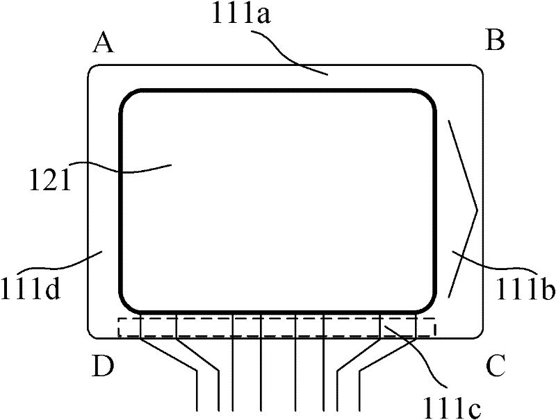
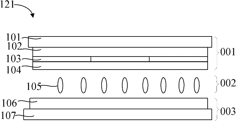
[0040] In order to solve the problems described in the background art, the inventor provides a touch display device, the touch display device includes a pixel array substrate and a touch screen substrate including a touch structure layer arranged oppositely; the display plane includes an image display And a touch-sensitive touch display area, and a peripheral lead area arranged with a plurality of leads (including scan line leads and common electrode leads); in the peripheral lead area, the touch display device includes: oppositely arranged touch screen substrates The first transparent substrate and the second transparent substrate of the pixel array substrate, the output leads of the touch structure, the shielding layer, the insulating layer, and the peripheral leads of the pixel array are sequentially arranged from the first transparent substrate to the second transparent substrate; The output lead of the structure includes a driving electrode lead and a sensing electrode lead. The shielding layer includes a first shielding layer and a second shielding layer. The first shielding layer is arranged between the driving electrode lead and the peripheral lead of the pixel array. The second shielding layer is arranged between the sensing electrode leads and the peripheral leads of the pixel array, and the first shielding layer and the second shielding layer are respectively electrically connected to the ground.
[0041] Combine below Figure 7 The shown schematic diagram of the touch equivalent circuit of the touch display device of the present invention describes the principle that the touch display device of the present invention can improve the signal to noise ratio.
[0042] Such as Figure 7 As shown, the equivalent circuit includes: a signal source 3, a driving electrode resistance 1, a sensing electrode resistance 2, a detection circuit 6, a mutual capacitance 12 between the driving electrode and the sensing electrode, and the equivalent circuit also includes a driving electrode lead The first parasitic capacitance 51 generated between the first shielding layer, the first shielding layer resistance 52 and the first shielding layer inductance 53, the second parasitic capacitance 54 generated between the sensing electrode lead and the second shielding layer, the second shielding layer The layer resistance 55 and the second shielding layer inductance 56; since the first shielding layer and the second shielding layer are electrically connected to the ground terminal, in the equivalent circuit, the first parasitic capacitance 51, the first shielding layer resistance 52 and the first shielding layer inductance 53 are connected in series and then connected to the ground 57, and the second parasitic capacitance 54, the second shielding layer resistance 55 and the second shielding layer inductance 56 are connected in series and then connected to the ground 57.
[0043] After the AC signal sent by the signal source 3 passes through the driving electrode resistor 1, part of the AC signal reaches the detection circuit 6 through the mutual capacitance 12 and the sensing electrode resistance 2, and part of the AC signal passes through the first parasitic capacitance 51, the first shielding layer resistance 52 and The first shielding layer inductance 53 leads to the ground 57, or the second parasitic capacitance 54, the second shielding layer resistance 55, and the second shielding layer inductance 56 lead to the ground 57. It is difficult for AC signals to pass through the first parasitic capacitance 51 and the second A shielding layer resistance 52, a first shielding layer inductance 53, a second parasitic capacitance 54, a second shielding layer resistance 55, and a second shielding layer inductance 56 are detected by the detection circuit 6, so that no large substrate is generated at the detection circuit The signal detected by the detection circuit 6 is mainly the detection signal through the mutual capacitance 12, so that the detection signal change caused by the change of the mutual capacitance 12 can be detected more accurately, thereby avoiding the detection failure problem caused by the large parasitic capacitance.
[0044] The technical solution of the present invention will be further described below in conjunction with specific embodiments.
[0045] reference Figure 8 , Shows a schematic diagram of an embodiment of the touch display device of the present invention. The touch display device is an LCD touch display. Its display plane includes a touch display area 211 and a peripheral lead area 212 surrounding the touch display area 211. The touch display area 211 of the touch display device includes a pixel array substrate 006 in the light transmission direction, a touch screen substrate 004 disposed opposite to the pixel array substrate 006, and a liquid crystal layer 005 disposed between the pixel array substrate 006 and the touch screen substrate 004 . The touch screen substrate 004 includes the first transparent substrate 201, the touch structure layer 202, the insulating layer 203, and the common electrode layer (ITO) 204 from the farthest closer to the liquid crystal layer 005; the liquid crystal layer 005 includes a plurality of liquid crystal molecules 205; pixels The array substrate 006 includes a pixel array 206 and a second transparent substrate 207 in order from the closest to the liquid crystal layer 005. When a color display is to be realized, a color filter (CF) can be used as the insulating layer 203, or a color filter can be added between the first transparent substrate 201 and the touch structure layer 202. The LCD touch display device also includes a polarizer, a backlight structure, etc., which are not shown in the figure for brevity and clarity.
[0046] In the peripheral lead area 212, the peripheral leads of the pixel array substrate 006 (including the common electrode leads and the scan line leads) overlap with the output leads (including the driving electrode leads and the sensing electrode leads) of the touch structure layer 202 of the touch screen substrate 004 The area is 212a. At the overlapping area 212a, the touch display device includes a first transparent substrate 201 and a second transparent substrate 207 disposed oppositely, and the touch structure layer is sequentially disposed from the first transparent substrate 201 to the second transparent substrate 207 The output lead 210 of 202, the shielding layer 209, the insulating layer 208, and the peripheral lead 220 of the pixel array 206.
[0047] Combined reference Picture 9 ,show Figure 8 The top view schematic diagram of the first embodiment of the touch screen substrate shown, in order to make the structure and position of the shielding layer clearer, Picture 9 Only the shielding layer 209, the touch structure layer 202, the output leads 210 of the touch structure layer 202, and the common electrode layer 204 are shown in FIG.
[0048] In this embodiment, a single-layer electrode touch structure layer is taken as an example. In the single-layer electrode touch structure layer, the driving electrode and the sensing electrode are located in the same layer. Specifically, at the touch display area 211, the touch The structure layer 202 includes: a plurality of driving electrodes 2021 arranged in columns, a plurality of strip-shaped sensing electrodes 2022, each column of driving electrodes 2021 and sensing electrodes 2022 are spaced apart, the driving electrodes 2021 and adjacent sensing electrodes 2022 form a mutual capacitance At the overlap area 212a between the peripheral leads of the pixel array substrate and the output leads 210 of the touch structure layer 202 of the touch screen substrate, the output leads 210 of the touch structure layer 202 include drive electrode leads 2023 and sense electrode leads 2024, The driving electrode 2021 is connected to a driving circuit (not shown) through a driving electrode lead 2023, and the sensing electrode 2022 is connected to a detection circuit (not shown) through a sensing electrode lead 2024.
[0049] In the overlap area 212a, the shielding layer 209 is the same layer and the same material as the common electrode layer 204 in the touch display area 211, so that the shielding layer 209 and the common electrode layer 204 can be prepared at the same time without additional preparation steps . Specifically, the material of the shielding layer 209 is indium tin oxide (ITO), and the thickness of the shielding layer 209 is between 1000 and 1500. In the range.
[0050] In this embodiment, the shielding layer 209 includes a first shielding layer 2091 and a second shielding layer 2092, and the first shielding layer 2091 and the second shielding layer 2092 are mutually independent rectangular conductive films arranged on the same layer. Wherein, the first shielding layer 2091 is disposed in the peripheral lead area 212a between the driving electrode lead 2023 and the peripheral lead (including the common electrode lead and the scan line lead) of the pixel array substrate, and is electrically connected to the ground; The second shielding layer 2092 is disposed in the peripheral lead area 212a between the sensing electrode lead 2024 and the peripheral lead (including the common electrode lead and the scan line lead) of the pixel array substrate, and is electrically connected to the ground.
[0051] Such as Picture 9 As shown, the common electrode layer 204 includes a plurality of first common electrodes 2041 and second common electrodes 2042 arranged at intervals; the first common electrode 2041 and the driving electrode 2021 are arranged opposite to each other in the light transmission direction, and the second common electrode 2042 and the sensing The electrodes 2022 are arranged directly opposite; all the first common electrodes 2041 are connected to the ground terminal 303 in parallel, and all the second common electrodes 2042 are connected to the ground terminal 304 in parallel. In this way, coupling of the driving electrode and the sensing electrode through the parasitic capacitance formed with the common electrode can be avoided, and the detection signal-to-noise ratio can be further improved.
[0052] In this embodiment, the first shielding layer 2091 is electrically connected to the first common electrode layer 2041 through a connecting wire (not shown), and then electrically connected to the ground terminal 303; the second shielding layer 2092 is electrically connected to the ground terminal 303 through a connecting wire (not shown) (Not shown) is electrically connected to the second transparent conductive layer 2042, and further electrically connected to the ground terminal 304. It should be noted that, in the first embodiment of the present invention, the first shielding layer 2091 can also be integrated with the first common electrode 2041, that is to say, the ITO used as the first common electrode 2041 extends to the peripheral lead area. , Covering the driving electrode lead 2023, the second shielding layer 2092 can also be integrated with the second common electrode 2042, that is to say, the ITO used as the second common electrode 2042 extends to the peripheral lead area, covering the sensing The electrode lead 2024.
[0053] It should also be noted that, in the first embodiment of the present invention, the common electrode includes a first common electrode 2041 and a second common electrode 2042. The first common electrode 2041 and the second common electrode 2042 are grounded, but the current The invention is not limited to this. The common electrode may be an integral common electrode, and one of the first shielding layer 2091 and the second shielding layer 2092 is connected to the ground through the common electrode, and is not grounded through the common electrode. The shield can be grounded through other components. In addition, the first shielding layer 2091 and the second shielding layer 2092 may not be connected to the ground through a common electrode, as long as the two are grounded separately, and those skilled in the art can make corresponding modifications, substitutions and deformations according to the above-mentioned embodiments.
[0054] The present invention also provides a second embodiment of the touch display device. The difference between this embodiment and the first embodiment is that the touch structure layer is a two-layer electrode touch structure, that is, the driving electrodes and the sensing electrodes are located in different layers, and An insulating layer is arranged between the driving electrode and the sensing electrode. reference Picture 10 ,show Figure 8 The top view of the second embodiment of the touch screen substrate in the touch display device is shown. The touch screen in the touch display device includes a driving electrode 401 and a sensing electrode 402. The driving electrode? 401 usually includes a plurality of driving electrodes arranged in rows, such as 6a, 6b, 6c, 6d, 6e, 6f, 6g, 6h, and the sensing electrode 402 usually includes a plurality of sensing electrodes arranged in columns, such as 5a , 5b, 5c, 5d, 5e, 5f, 5g, 5h. The driving electrode and the sensing electrode overlap each other to form a mutual capacitance.
[0055] Wherein, there are output leads in the peripheral lead area of ​​the touch display device, including driving electrode leads 405 and sensing electrode leads 406. The driving electrode leads 405 are used to connect the driving electrode 401 to the driving circuit (not shown). The electrode lead 406 is used to connect the sensing electrode 402 to a detection circuit (not shown). Since the driving electrode leads 405 (sensing electrode leads 406) and the peripheral leads of the pixel array (such as scan line leads or common electrode leads) overlap, a large mutual capacitance will be generated. The touch display device is also provided in the peripheral lead area. The first shielding layer 403 and the second shielding layer 404 are arranged between the driving electrode lead 405 and the peripheral leads of the pixel array, and the second shielding layer 404 is connected to the ground and arranged at the sensor Between the electrode lead 406 and the peripheral lead of the pixel array, the first shielding layer 403 and the second shielding layer 404 are respectively electrically connected to the ground.
[0056] Correspondingly, the present invention also provides a manufacturing method including the above touch display device, and the method includes the following steps:
[0057] Provide a first transparent substrate;
[0058] A touch structure layer and output leads of the touch structure layer are formed on the first transparent substrate. The touch structure layer is a single-layer electrode touch structure, including drive electrodes and sensing electrodes arranged at intervals; a touch structure layer The output leads include driving electrode leads and sensing electrode leads;
[0059] Attaching a color filter to the touch screen;
[0060] A common electrode layer is deposited on the color filter, and spaced first and second common electrodes are formed in the display area of ​​the touch display device. The first common electrode and the driving electrode are arranged directly opposite to each other. The second common electrode and the sensing electrode are arranged directly opposite;
[0061] In the process of forming the first common electrode and the second common electrode, a first shielding layer covering the driving electrode lead and connected to the first common electrode and a first shielding layer covering the sensing electrode lead and connected to the second common electrode are formed. The second shielding layer connected to the electrode;
[0062] Providing a second transparent substrate and forming a pixel array thereon;
[0063] A liquid crystal layer is formed between the first transparent substrate and the second transparent substrate, and is attached to the first transparent substrate and the second transparent substrate.
[0064] It should be noted that in the above-mentioned manufacturing method of the touch display device, the shielding layer and the common electrode layer are the same transparent conductive material (ITO). Therefore, the common electrode layer can be formed in the display area while the shielding is formed in the peripheral lead area. Therefore, the manufacturing of the touch display device of the present invention does not increase the process steps, but the present invention is not limited to this. The shielding layer may also be other conductive materials. Since the shielding layer is located in the peripheral lead area, the shielding The layer can be made of conductive materials such as opaque metal.
[0065] It should also be noted that in the above embodiments, the shielding layer is provided in the touch screen substrate, but the present invention is not limited to this. The shielding layer can also be provided in the pixel array substrate. It should also be noted that the above In the embodiments, a liquid crystal display device is taken as an example, but the present invention is not limited to this. It may also be an organic electroluminescent diode (OLED) display device. Those skilled in the art can make corresponding deformations, modifications, and modifications according to the above-mentioned embodiments. replace.
[0066] Although the present invention has been disclosed as above in preferred embodiments, it is not intended to limit the present invention. Any person skilled in the art can use the methods and technical content disclosed above to improve the present invention without departing from the spirit and scope of the present invention. The technical solution makes possible changes and modifications. Therefore, all simple modifications, equivalent changes and modifications made to the above embodiments according to the technical essence of the present invention without departing from the content of the technical solution of the present invention belong to the technical solution of the present invention. protected range.

PUM

no PUM

Description & Claims & Application Information

We can also present the details of the Description, Claims and Application information to help users get a comprehensive understanding of the technical details of the patent, such as background art, summary of invention, brief description of drawings, description of embodiments, and other original content. On the other hand, users can also determine the specific scope of protection of the technology through the list of claims; as well as understand the changes in the life cycle of the technology with the presentation of the patent timeline. Login to view more.

Similar technology patents

Multi-wavelength Brillouin optical time domain analyzer

InactiveCN103115632AIncrease total optical powerImprove signal-to-noise ratioSpecial purpose recording/indication apparatusOptical pathSignal-to-noise ratio (imaging)
Owner:NANJING UNIVERSTIY SUZHOU HIGH TECH INST +1

Classification and recommendation of technical efficacy words

  • Improve signal-to-noise ratio

Magnetic tape, its cleaning method, and optical servotrack forming/cleaning apparatus

InactiveUS7803471B1Improve signal-to-noise ratioDecreasing rate of fluctuationMagnetic materials for record carriersReconditioning/cleaning record carriersReflectivityMaximum rate
Owner:FUJIFILM CORP

System for generating thermographic images using thermographic signal reconstruction

ActiveUS20050008215A1Reduce size and complexityImprove signal-to-noise ratioCharacter and pattern recognitionMaterial flaws investigationSignal reconstructionThermographic imaging
Owner:THERMAL WAVE IMAGING

Hyper-spectral imaging methods and devices

InactiveUS20050270528A1Improve signal to noise ratioSmall bandwidthRadiation pyrometrySpectrum generation using diffraction elementsSpectral imagingLight spectrum
Owner:PLAIN SIGHT SYST
Why Eureka
Try Eureka