
Nand FLASH intelligent detection method based on ARM controller

An ARM controller, intelligent detection technology, applied in instruments, static memory and other directions, can solve the problems of FLASH damage, reduced product life, poor flexibility, etc., to achieve good pin compatibility, short instruction cycle, high execution efficiency Effect

Active Publication Date: 2015-01-21
雷智数系统技术西安有限公司
View PDF2 Cites 0 Cited by
  • Summary
  • Abstract
  • Description
  • Claims
  • Application Information

AI Technical Summary

Problems solved by technology

The former is more complicated to implement, and the flexibility is not good, and it needs to complete the writing of the upper computer software. The latter method is more convenient to detect, but it needs frequent replacement of Nand FLASH and mass production of Nand FLASH
It itself will damage the FLASH, which will directly reduce the life of the product

Method used


Image

  • Nand FLASH intelligent detection method based on ARM controller

Examples


Embodiment Construction

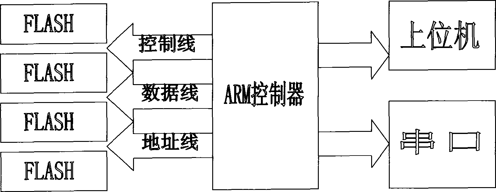
[0030] see figure 1 ,

[0031] 1) First, group the GPIOs of the main control ARM, corresponding to the data bus, address bus and control bus of the flash memory chip (Nand FLASH), and perform register configuration.

[0032] 2) Use the GPIO of the main control to simulate the read and write timing of Nand FLASH, and read the chip ID and bad block information of the flash memory chip.

[0033] 3) Sort out a data list to store the bad chip judgment criteria of each Nand FLASH, specifically the number of bad blocks in the chip.

[0034] 4) Compare the number of detected bad blocks with the corresponding value in the data list to determine whether it is a bad block.

[0035] The present invention is characterized in that:

[0036] The choice of ARM and the flexible configuration of GPIO, the flexible configuration of GPIO into three buses, each bus can be flexibly configured into different circuit characteristics;

[0037] Secondly, the optimized data structure defines a struc...


PUM


Abstract

The invention relates to an Nand FLASH intelligent detection method based on an ARM controller, comprising the following steps of: 1) dividing GPIOs (general purpose inputs / outputs) of a master control ARM into groups which are respectively corresponding to a data bus, an address bus and a control bus of an Nand FLASH, and configuring; 2) simulating read-write time sequence of the Nand FLASH with GPIOs of the master control ARM, and reading chip ID and bad block information of the Nand FLASH by an ARM controller; 3) sorting out a data list by the ARM controller, and taking number of the bad blocks in the Nand FLASH as the bad block judgement standard; and 4) comparing the number of the detected bad blocks with a corresponding value in the data list, and judging whether to be a bad Nand FLASH or not. The Nand FLASH intelligent detection method based on the ARM controller provided by the invention has the advantages that a hardware circuit is simple and stable, few peripheral circuits are used, instruction operation is fast, multiple Nand FLASHes can be detected at one time, no driving circuit is required to be added additionally, software codes are less, execution efficiency is high, types of compatible chips are multiple and a new chip can be compatible only requiring a small code change after the new chip is produced.

Description

technical field [0001] The invention relates to an intelligent detection method of Nand FLASH based on an ARM controller. It specifically relates to an intelligent detection of ID information, bad block number, and electrical characteristics of Nand FLASH through a low-cost ARM controller. Background technique [0002] The full name of FLASH is FLASH Memory, which is a non-volatile memory device (Non-volatile Memory Device), and corresponds to a volatile memory device (Volatile Memory Device). Nand FLASH is a widely used type of FLASH. In the design of Nand FLASH, reading the ID means reading the ID information of the chip. The ID read here reads multiple bytes, generally at least 4 , the new chip supports 5 or more bytes, and a lot of relevant information can be parsed out from these bytes. At the same time, reading out the data in the area specified by the manufacturer can detect bad block information. [0003] Commonly used Nand FLASH detection is completed based on FP...

Claims


Application Information

Patent Timeline
Patent Type & Authority Patents(China)
IPC IPC(8): G11C29/56
Inventor 刘升雒宵
Owner 雷智数系统技术西安有限公司
Learn More