Forming method of graph of aligned layer on silicon chip

A technology for aligning layers and silicon wafers, applied in the manufacture of electrical components, electrical solid devices, semiconductor/solid devices, etc., can solve the problems of long manufacturing time and increased process costs, and achieve the effect of contrast enhancement

Active Publication Date: 2012-07-04
SHANGHAI HUAHONG GRACE SEMICON MFG CORP
View PDF4 Cites 8 Cited by
  • Summary
  • Abstract
  • Description
  • Claims
  • Application Information

AI Technical Summary

Problems solved by technology

[0014] The method for forming the pattern of the aligned layer on the silicon wafer requires two photolithography processes, which increases the cost of the process and makes the manufacturing time longer

Method used


Image

  • Forming method of graph of aligned layer on silicon chip
  • Forming method of graph of aligned layer on silicon chip
  • Forming method of graph of aligned layer on silicon chip

Examples


Embodiment Construction

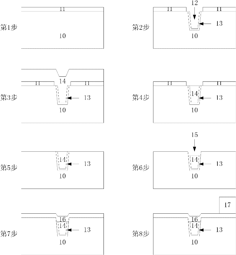
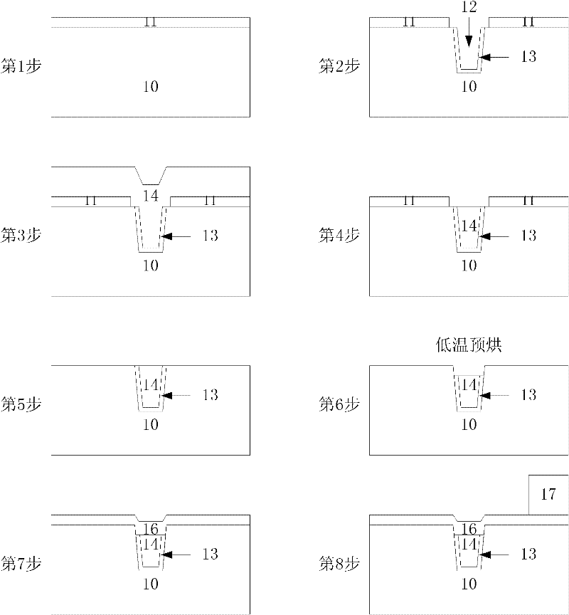
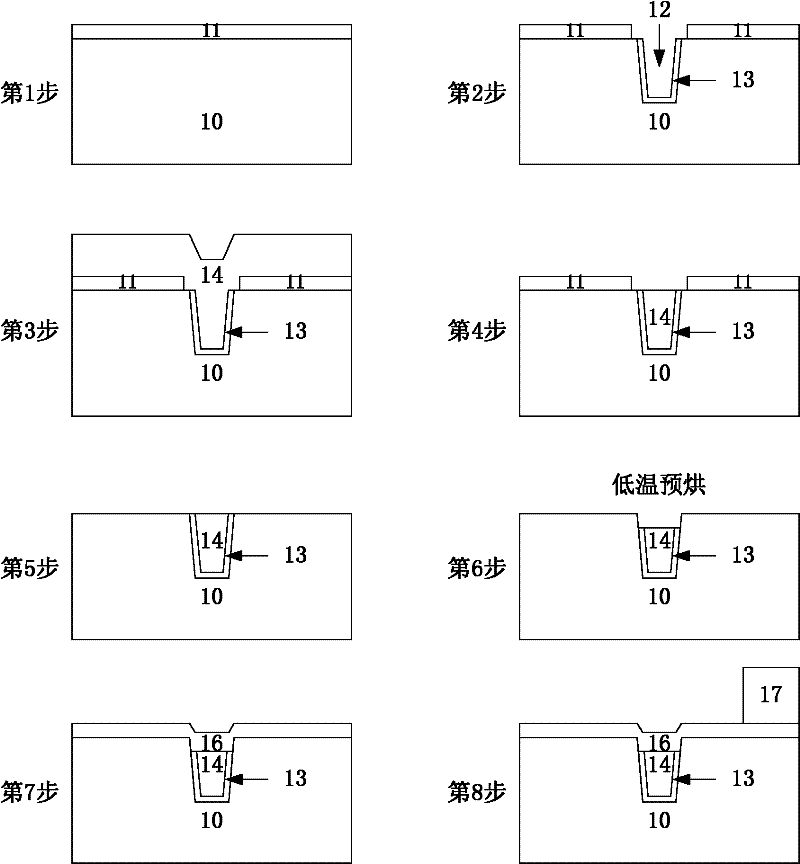
[0030] see figure 2 The method for forming the pattern of the aligned layer on the silicon wafer of the present invention comprises the following steps:

[0031] In the first step, a first dielectric layer 11, such as silicon nitride, is deposited on the substrate 10.

[0032] In the second step, a trench 12 is etched on the substrate 10 by photolithography and etching processes, and after the etching is completed, the photoresist is removed, and a pad oxide layer is grown on the bottom and side walls of the trench 12 ( Liner Oxide) 13. A shallow trench isolation (STI) process may be used to etch the trench 12 .

[0033] The groove 12 is used as an overlay mark of this layer of graphics on the silicon wafer, and the overlay mark may be a line or shape (such as a square ring, a cross, etc.) from a top view of the silicon wafer, but from a cross-sectional view of the silicon wafer It's the groove. The aligned layer pattern is a silicon wafer pattern formed on the basis of o...


PUM


Abstract

The invention discloses a forming method of a graph of an aligned layer on a silicon chip. Compared with the prior art, the forming method is characterized in that the steps of secondary photoetching and etching are omitted, and a way of performing low-temperature pretreatment on the silicon chip is adopted in the forming method, so that the single contrast of the graph of an overlay target of the graph of the aligned layer is enhanced, and the graph is easier and clearer to be recognized.

Description

technical field [0001] The invention relates to a method for forming an aligned layer pattern in a photolithography process. Background technique [0002] Photolithography is a process of transferring the circuit structure in the form of a pattern on a mask to the surface of a silicon wafer coated with photoresist through steps such as alignment, exposure, and development. The photolithography process will form a layer of photoresist mask pattern (photolithography pattern) on the surface of the silicon wafer, and its subsequent process is etching or ion implantation. [0003] The manufacture of any semiconductor device includes a multi-step photolithography process. In addition to the first step of photolithography, the photolithography pattern of the current layer must be overlaid with the aligned layer pattern of the previous layer in each step of photolithography. , to ensure alignment of patterns on silicon wafers between multiple photolithographic steps. The pattern o...

Claims


Application Information

Patent Timeline
IPC IPC(8): H01L21/02H01L21/027H01L23/544
Inventor 孟鸿林王雷缪燕郭晓波
Owner SHANGHAI HUAHONG GRACE SEMICON MFG CORP
Why Eureka
Try Eureka