Etching method and etching device for mask layer and etching method for interlayer dielectric layer

A technology of interlayer dielectric layer and mask layer, which is applied in the direction of electrical components, semiconductor/solid-state device manufacturing, circuits, etc., can solve problems such as time-consuming and cost-consuming, difficulty in exciting radio frequency and biasing radio frequency, etc., to avoid insufficient kinetic energy, Effect of suppressing damage results and low cost

Active Publication Date: 2012-07-04
ADVANCED MICRO FAB EQUIP INC CHINA
View PDF2 Cites 12 Cited by
  • Summary
  • Abstract
  • Description
  • Claims
  • Application Information

AI Technical Summary

Problems solved by technology

[0008] The problem solved by the present invention is to propose a new mask layer etching method to solve the problem of finding suitable excitation radio frequency and bias radio frequency power in the prior art, but it is difficult to obtain the appropriate excitation radio frequency and bias radio frequency. time consuming and costly

Method used


Image

  • Etching method and etching device for mask layer and etching method for interlayer dielectric layer
  • Etching method and etching device for mask layer and etching method for interlayer dielectric layer
  • Etching method and etching device for mask layer and etching method for interlayer dielectric layer

Examples


Embodiment 1

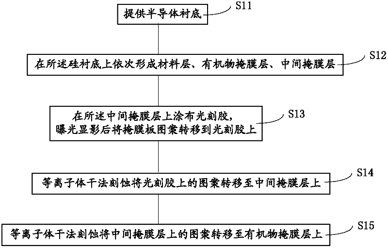
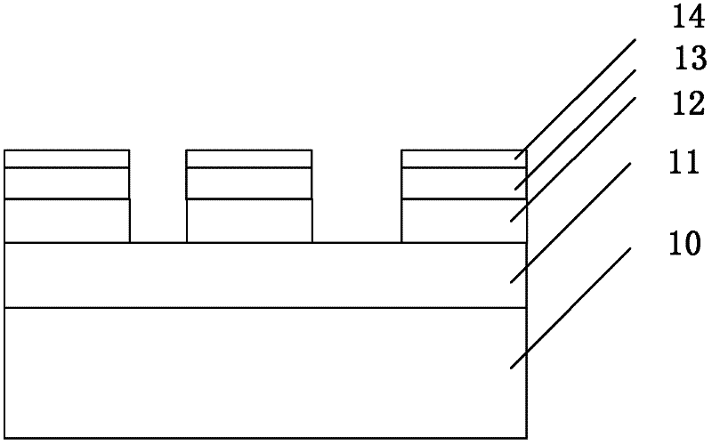
[0047] figure 1 It is a flow chart of the etching method of the mask layer provided in the first embodiment, figure 2 It is a schematic diagram of the final structure after the method is executed. The following combination figure 1 and figure 2 , which details the method.

[0048] First, step S11 is performed to provide a semiconductor substrate; in the first embodiment, the semiconductor substrate is a silicon substrate 10 , and germanium can also be selected as required.

[0049] Next, step S12 is performed to sequentially form a material layer, an organic mask layer, and an intermediate mask layer on the silicon substrate 10 .

[0050] The material layer can be metal, dielectric layer or silicon. In the first embodiment, the interlayer dielectric layer 11 is taken as an example. The material of the interlayer dielectric layer 11 is silicon-containing inorganic material, which can be used to form trenches in subsequent processes. .

[0051] In the first embodiment, t...

Embodiment 2

[0069] The second embodiment provides a method for etching an interlayer dielectric layer, such as Figure 4 As shown, after the steps S11-S15 in the first embodiment are executed, step S16 is then executed to etch the underlying interlayer dielectric layer 11 using the patterned organic mask layer as a mask. In the second embodiment, the organic mask layer follows the amorphous carbon layer 12 of the first embodiment.

[0070] The etching process in this step can use plasma dry etching, and in this process, plasma radio frequency excitation voltage is applied to generate plasma. The frequency range of the plasma excitation radio frequency voltage includes: 20MHz to 120MHz, which can be specifically determined according to the Plasma concentration and distribution requirements to adjust. In addition, this step can also use an existing process.


PUM


Abstract

The invention discloses an etching method for a mask layer. The mask layer at least comprises a middle mask layer and an organic matter mask layer; the mask layer is etched with a plasma dry process; and in an etching process, a plasma radiofrequency excitation voltage is applied to generate plasma. The etching of the mask layer comprises the following steps of: forming a patterned middle mask layer by taking a patterned photoresist layer as a middle mask layer below mask etching; and applying a pulse bias radiofrequency voltage, and forming a patterned organic matter mask layer by taking the patterned middle mask layer as an organic matter mask layer below mask etching, wherein the frequency of the plasma radiofrequency excitation voltage is higher than that of the pulse bias radiofrequency voltage. The invention further provides an etching device for the mask layer and an etching method for an interlayer dielectric layer. Due to the adoption of the technical scheme provided by the invention, an implementation condition is simple and cost is low.

Description

technical field [0001] The invention relates to the field of semiconductor manufacturing, in particular to an etching method and an etching device for a mask layer. In addition, the invention also relates to an etching method for an interlayer dielectric layer. Background technique [0002] In the semiconductor integrated circuit manufacturing process, a semiconductor structure is formed on a semiconductor substrate through a series of processes, such as deposition, photolithography, etching, planarization and other processes. Wherein, a photolithography process is used to form a mask pattern to define a region to be etched. The etching process is used to transfer the pattern defined by lithography to the material (metal, dielectric layer or silicon) to form the desired structure. The pattern is transferred to the hard mask, and then the pattern is transferred to the material (metal, dielectric layer or silicon) using the patterned hard mask as a mask. [0003] The transfe...

Claims


Application Information

Patent Timeline
Patent Type & Authority Applications(China)
IPC IPC(8): H01L21/033H01L21/311
Inventor 凯文皮尔斯
Owner ADVANCED MICRO FAB EQUIP INC CHINA
Why Eureka
Try Eureka