
Protection device against electromagnetic interference

A protection device, protection circuit technology, applied in the direction of circuit device, crosstalk/noise/electromagnetic interference reduction (, printed circuit, etc.) , to achieve the effect of improving aging performance, small structure height and good filtering quality

Inactive Publication Date: 2012-07-04
ROBERT BOSCH GMBH
View PDF5 Cites 0 Cited by
  • Summary
  • Abstract
  • Description
  • Claims
  • Application Information

AI Technical Summary

Problems solved by technology

Capacitors are dimensioned empirically, but in practice this can often lead to a non-optimal design of the guard wiring
Furthermore, a certain degradation performance was observed, i.e. a reduction in capacitance and a consequent loss of blocking capability due to multiple pulse loads
In addition to this effect, the parasitic series inductance prevents the rapid flow of carriers along the coupled input with the pulse, thereby degrading the filter characteristics of the device

Method used

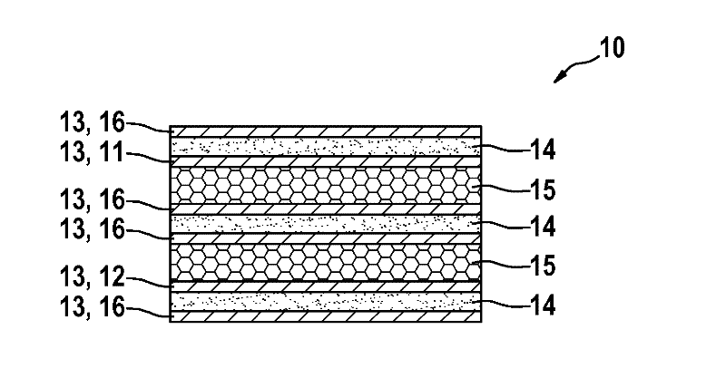
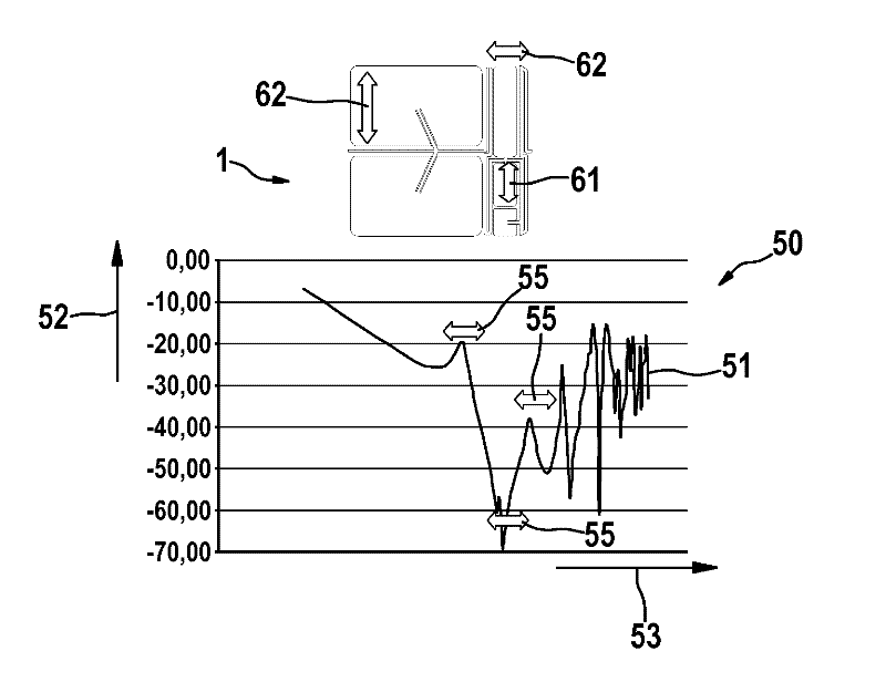
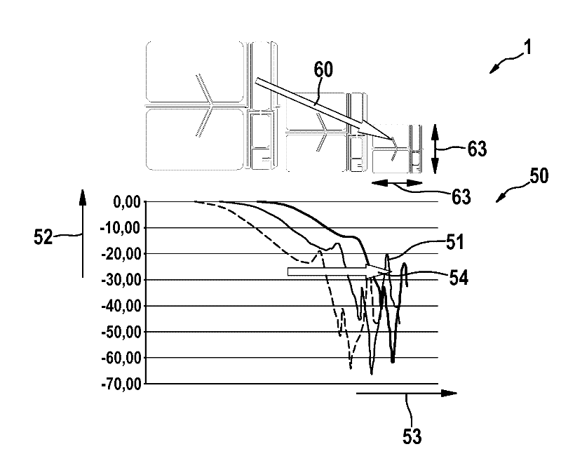

Image

  • Protection device against electromagnetic interference
  • Protection device against electromagnetic interference
  • Protection device against electromagnetic interference

Examples


Embodiment Construction

[0023] exist figure 1 A protective device 1 with capacitive and inductive structures 30 , 20 forming a protective circuit 40 is shown in plan view, wherein the capacitive structure 30 according to the invention is shown as an embedded component in a printed circuit board. In this view, therefore, only the electrodes 11 , 12 of the capacitive structures 30 and the conductor tracks coupling the capacitive structures 30 to one another can be seen. The conductor tracks form the inductive structure 20 here. In this illustration, the corresponding corresponding electrodes or shields and insulating or dielectric layers are not shown. These are located as additional coatings invisibly below and / or above the illustrated coatings.

[0024] In the example shown, a first capacitor 31 is shown, which, viewed in the signal direction, is arranged directly after the input 41 of the protective circuit 40 and assumes relatively large values ​​depending on the area of ​​the structure. In the ...


PUM


Abstract

The invention relates to a protection device for reducing grid-bound interference, comprising a protection circuit as an input filter of an electronic circuit, wherein the electronic circuit is applied to a multilayer circuit board or is at least partially integrated therein, wherein individual components of the circuit are implemented as embedded structures in the multilayer circuit board. According to the invention, the protection circuit is formed by a cascade of at least two capacitances coupled to each other by means of low-inductance circuit board structures, wherein the capacitances are implemented as embedded capacitor structures on or within the multilayer circuit board.; By means of said protection device, improved filter behavior can be achieved relative to discretely populated protection filters, in particular at higher frequencies, leading to improved protection against electrostatic interference. The filter structure can further be adjusted very well in simulation to the required interference resistance of the circuit to be protected, and also achieve improved aging behavior.

Description

Technical field [0001] The present invention involves a protective device used to reduce cablebundn interference. The protection device has a protective circuit as an input filter as an electronic circuit. Among themAmong the multi -layer printing circuit boards, each component of the circuit is implemented in an embedded structure in a multi -layer printing circuit board. Background technique [0002] For example, the wired interference of electrostatic discharge (ESD) may be coupled and entered into electronic components and damaged these electronic components.In order to protect these circuits, the so -called abbblockstrukturen constructed by mostly separated components is adopted. [0003] The example of this is a variable resistor, resistance related to voltage, or spark gaps at the beginning of the coupling input path that is arranged to protect the circuit to be protected.These are usually expensive and partially have large location needs.In addition, the SMD capacitor pla...

Claims


Application Information

Patent Timeline
Patent Type & Authority Applications(China)
IPC IPC(8): H05K1/16
CPCH05K1/0231H05K1/165H05K2201/09263H05K1/0233H05K1/162
Inventor C.斯普拉特勒
Owner ROBERT BOSCH GMBH
Learn More