Array substrate of thin film transistor (TFT)-liquid crystal display (LCD) and manufacture method thereof

The technology of an array substrate and manufacturing method, which is applied in the field of liquid crystal displays, can solve the problems of poor process realizability and low pixel transmittance, and achieve the effects of lower alignment accuracy requirements, optimized arrangement mode, and good process realizability

Active Publication Date: 2012-07-11
BOE TECH GRP CO LTD +1
View PDF5 Cites 10 Cited by
  • Summary
  • Abstract
  • Description
  • Claims
  • Application Information

AI Technical Summary

Problems solved by technology

[0006] When realizing the technical solution of the present invention, the inventors found that the array substrates of TFT-LCDs in the planar electric field mode provided by the prior art all have the defects of poor process realization and low pixel transmittance when high alignment accuracy is required.

Method used


Image

  • Array substrate of thin film transistor (TFT)-liquid crystal display (LCD) and manufacture method thereof
  • Array substrate of thin film transistor (TFT)-liquid crystal display (LCD) and manufacture method thereof
  • Array substrate of thin film transistor (TFT)-liquid crystal display (LCD) and manufacture method thereof

Examples


Embodiment 1

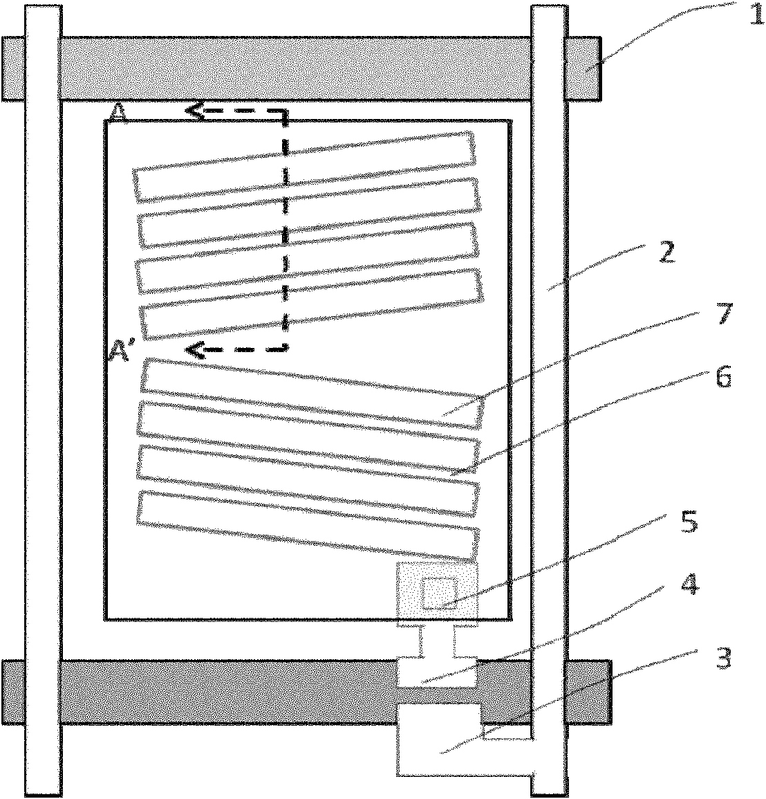
[0043] An embodiment of the present invention provides an array substrate of a TFT-LCD, such as Figure 5 with Image 6 As shown, the array substrate includes: a substrate, a gate line 1 and a data line 2 formed on the substrate; the intersection of the gate line 1 and the data line 2 defines a pixel unit, and each pixel unit includes a thin film transistor, a common electrode, a first pixel an electrode layer and a second pixel electrode layer;

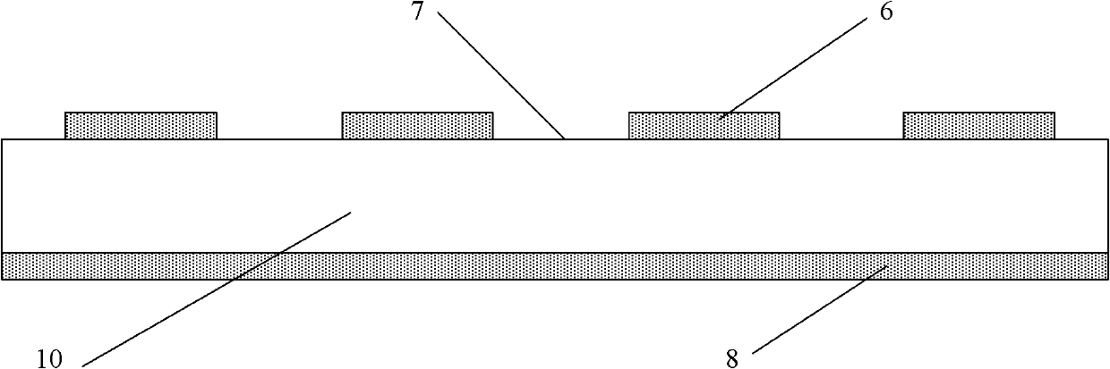
[0044] The first pixel electrode layer is separated from the second pixel electrode layer by an insulating layer 10; the first pixel electrode layer is connected to a common electrode, and includes several first pixel electrode layers separated by openings 9 of the first pixel electrode layer. The pixel electrode 8; the second pixel electrode layer is connected to the drain 4 of the thin film transistor through the drain contact hole 5, including several second pixel electrodes 6 separated by the second pixel electrode layer opening...

Embodiment 2

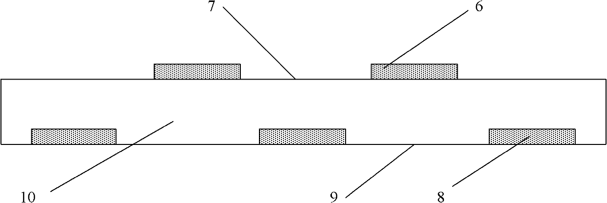
[0052] Such as Figure 7 As shown, there are two overlapping pixel electrodes 61 between the pixel electrodes 62 at two adjacent openings of the second pixel electrode layer. A first pixel electrode 8 is formed on the first pixel electrode layer, which has a width a, and an opening is formed on the first pixel electrode layer, which is the first pixel electrode layer opening 9, which has a width b. The second pixel electrode layer forms a second pixel electrode 6 with a width c, and an opening is formed on the second pixel electrode layer, which is a second pixel electrode layer opening 7 with a width d. Make the two edges of one first pixel electrode 8 of the second pixel electrode layer completely fall within one opening of the first pixel electrode layer. Then the relationship between the width a of the first pixel electrode of the first pixel electrode layer, the opening width b of the first pixel electrode layer, the width c of the second pixel electrode of the second pi...

Embodiment 3

[0056] The embodiment of the present invention also provides a method for manufacturing the array substrate of the TFT-LCD described in the above embodiment, such as Figure 8 As shown, the method includes:

[0057] Step 101, depositing a thin film of the first pixel electrode layer, forming a pattern including the first pixel electrode layer through a patterning process, and the first pixel electrode layer includes several first pixel electrodes separated by openings in the first pixel electrode layer, so The pattern of the first pixel electrode layer is connected to the common electrode;

[0058] Further, the metal layer thin film of the gate line is deposited, and the pattern including the gate line, the gate electrode, and the common electrode is formed through a patterning process, and the pattern of the first pixel electrode layer is connected to the common electrode; the first insulating layer is deposited, and the The source-drain metal layer film is formed by a patte...


PUM

PropertyMeasurementUnit
widthaaaaaaaaaa

Abstract

An embodiment of the invention discloses an array substrate of a thin film transistor (TFT)-liquid crystal display (LCD) and a manufacture method thereof, which relate to the technical field of liquid crystal displays and can reduce storage capacity when aligning accuracy is not high. The array substrate comprises a substrate, grid lines and data lines, wherein the grid lines and the data lines are arranged on the substrate. Each grid line and each data line intersect to define a pixel unit which comprises the TFT, a pubic electrode, a first pixel electrode layer and a second pixel electrode layer, wherein the first pixel electrode layer and the second pixel electrode layer are separated by an insulation layer. The first pixel electrode layer is connected with the pubic electrode and comprises a plurality of first pixel electrodes separated by first pixel electrode layer openings. The second pixel electrode layer is connected with a drain electrode of the TFT and comprises a plurality of second pixel electrodes separated by second pixel electrode layer openings. The second pixel electrode comprises overlaying-position pixel electrodes completely overlaid on the first pixel electrodes and opening-position pixel electrodes with edges completely in the first pixel electrode layer openings.

Description

technical field [0001] The invention relates to the field of liquid crystal displays, in particular to a thin film transistor liquid crystal display (Thin Film Transistor-Liquid Crystal Display, TFT-LCD for short) array substrate and a manufacturing method thereof. Background technique [0002] Among liquid crystal displays of TN, IPS, VA and planar electric field modes, the planar electric field mode has the advantages of wide viewing angle, low chromatic aberration, and high transmittance, and is increasingly adopted by major panel manufacturers. [0003] However, the process sequence of the planar electric field mode thin film transistor liquid crystal display in the array process section is different from that of other modes of liquid crystal displays. Such as figure 1 with figure 2 In the array substrate structure shown, the intersection of the gate line 1 and the data line 2 defines a pixel unit. During the manufacturing process, the first layer is the first pixel e...

Claims


Application Information

Patent Timeline
Patent Type & Authority Applications(China)
IPC IPC(8): G02F1/1343G02F1/1362G02F1/1368H01L27/12H01L21/77
CPCG02F2201/15G02F1/134363G02F2201/121G02F2201/122
Inventor 孙荣阁
Owner BOE TECH GRP CO LTD
Why Eureka
Try Eureka