

Surface-capacitive touch panel and manufacturing method thereof
A technology of surface capacitance and touch panel, which is applied in the direction of electrical digital data processing, instrumentation, data processing input/output process, etc., can solve the problem of thickness increase, etc., to reduce the film thickness, avoid the problem of excessive width of the front edge of the panel, Effect of improving film thickness uniformity
- Summary
- Abstract
- Description
- Claims
- Application Information
AI Technical Summary
Problems solved by technology
Method used
Image

Examples
Embodiment Construction
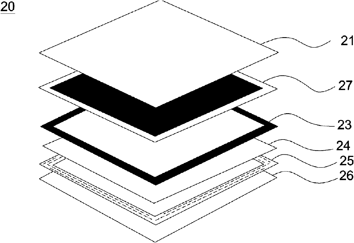
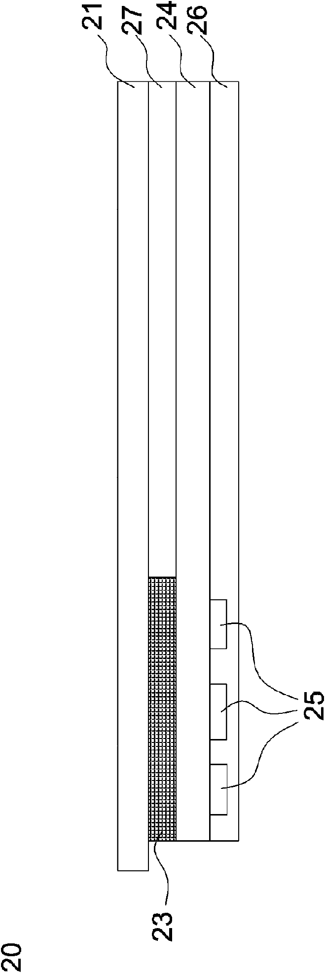
[0038] Figure 2A is an exploded view of components of a surface capacitive touch panel according to an embodiment of the present invention, Figure 2B for Figure 2A Schematic cross-sectional view of assembled components. Such as Figure 2A and Figure 2B As shown, the surface capacitive touch panel 20 at least includes a transparent substrate 21, a decoration layer 23, a capacitive sensing electrode layer 24 and a metal wiring pattern layer 25, the decoration layer 23 is formed on a surface of the transparent substrate 21 The capacitive sensing electrode layer 24 is formed on the first side of the transparent substrate 21 , and the metal wiring pattern layer 25 is formed on the capacitive sensing electrode layer 24 . For example, the capacitive sensing electrode layer 24 may include a plurality of first-axis sensing pads, a plurality of second-axis sensing pads, and a plurality of bridge lines connected between the sensing pads. A protection layer 26 is formed on the me...
PUM
| Property | Measurement | Unit |
|---|---|---|
| Film thickness | aaaaa | aaaaa |
| Film thickness | aaaaa | aaaaa |
Abstract
Description
Claims
Application Information