Intermetallic compound filled vertical through-hole interconnecting structure for three-dimensional package and preparation method thereof

A technology of intermetallic compounds and three-dimensional packaging, which is applied in semiconductor/solid-state device manufacturing, semiconductor/solid-state device components, semiconductor devices, etc., can solve the problems of poor conductivity of solder, low melting point of solder, poor conductivity, etc., and achieve the goal of manufacturing The process is convenient, the pass rate is improved, and the production cost is reduced.

Active Publication Date: 2012-07-11
NAT CENT FOR ADVANCED PACKAGING
View PDF4 Cites 22 Cited by
  • Summary
  • Abstract
  • Description
  • Claims
  • Application Information

AI Technical Summary

Problems solved by technology

(References Ko Y.-K., Fujii H.T., Sato Y.S., Lee C.-W., and Yoo S. Microelectron Eng 2012; 89:62-64.) But the disadvantage is that the solder has poor conductivity, and silicon The CTE (Coefficient of thermal expansion, coefficient of thermal expansion) of the materials is quite different, causing stress problems, and the melting point of the solder is low, which will cause many problems in the subsequent process
Filling with conductive glue can also simplify the filling process, but the conductivity is poor and it is difficult to fill holes with small diameters

Method used


Image

  • Intermetallic compound filled vertical through-hole interconnecting structure for three-dimensional package and preparation method thereof
  • Intermetallic compound filled vertical through-hole interconnecting structure for three-dimensional package and preparation method thereof
  • Intermetallic compound filled vertical through-hole interconnecting structure for three-dimensional package and preparation method thereof

Examples


Embodiment Construction

[0043] The present invention will be further described below in conjunction with specific drawings and embodiments.

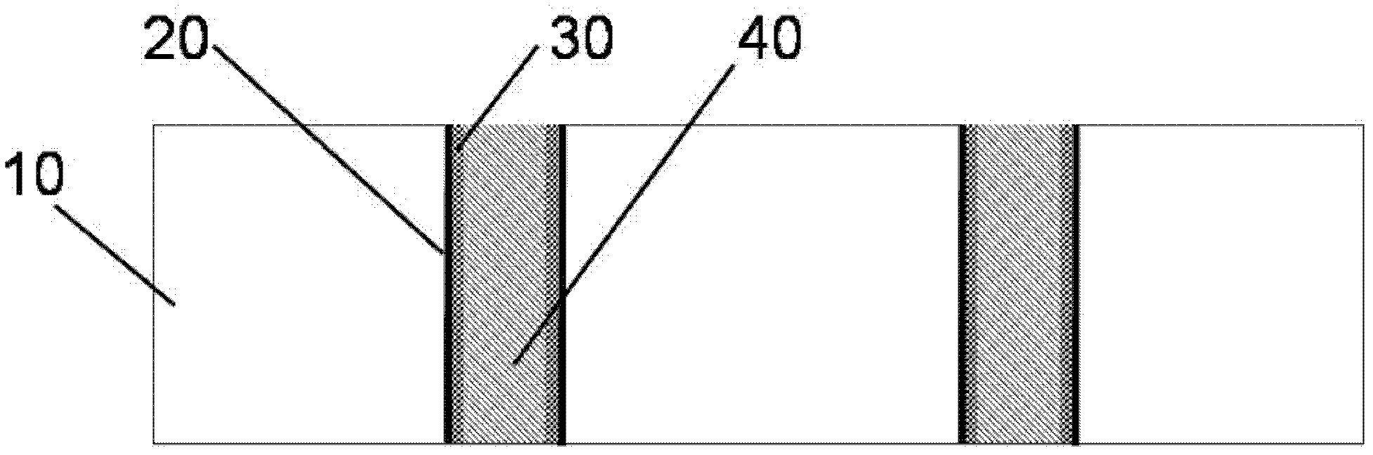
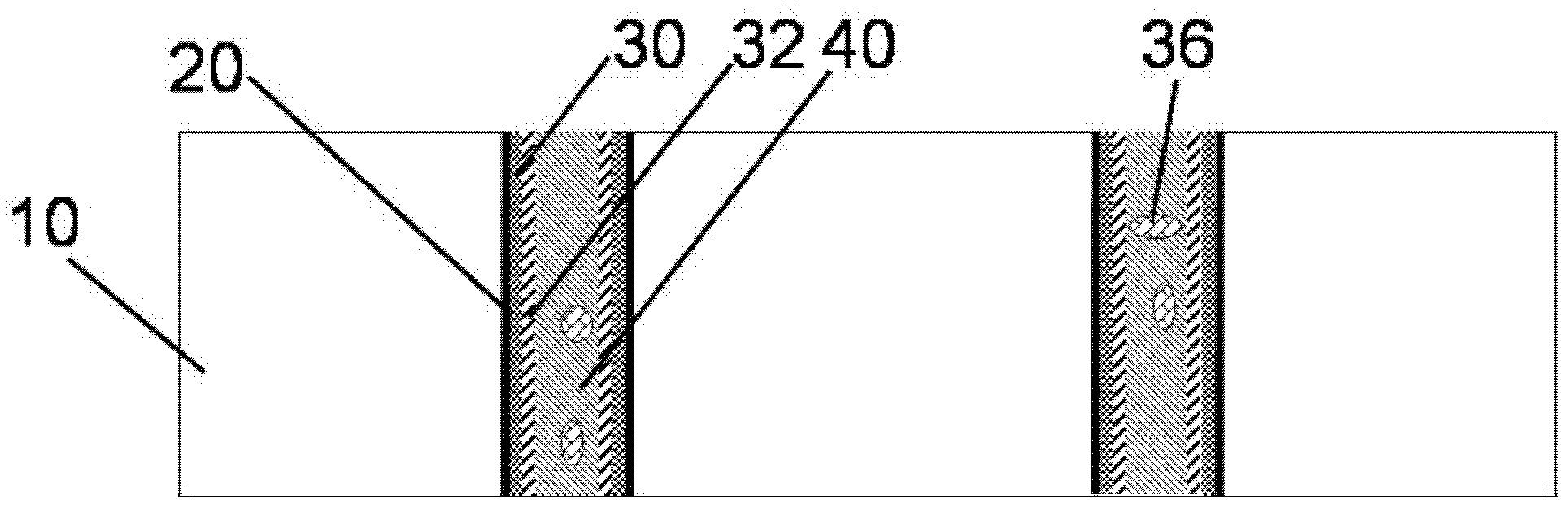
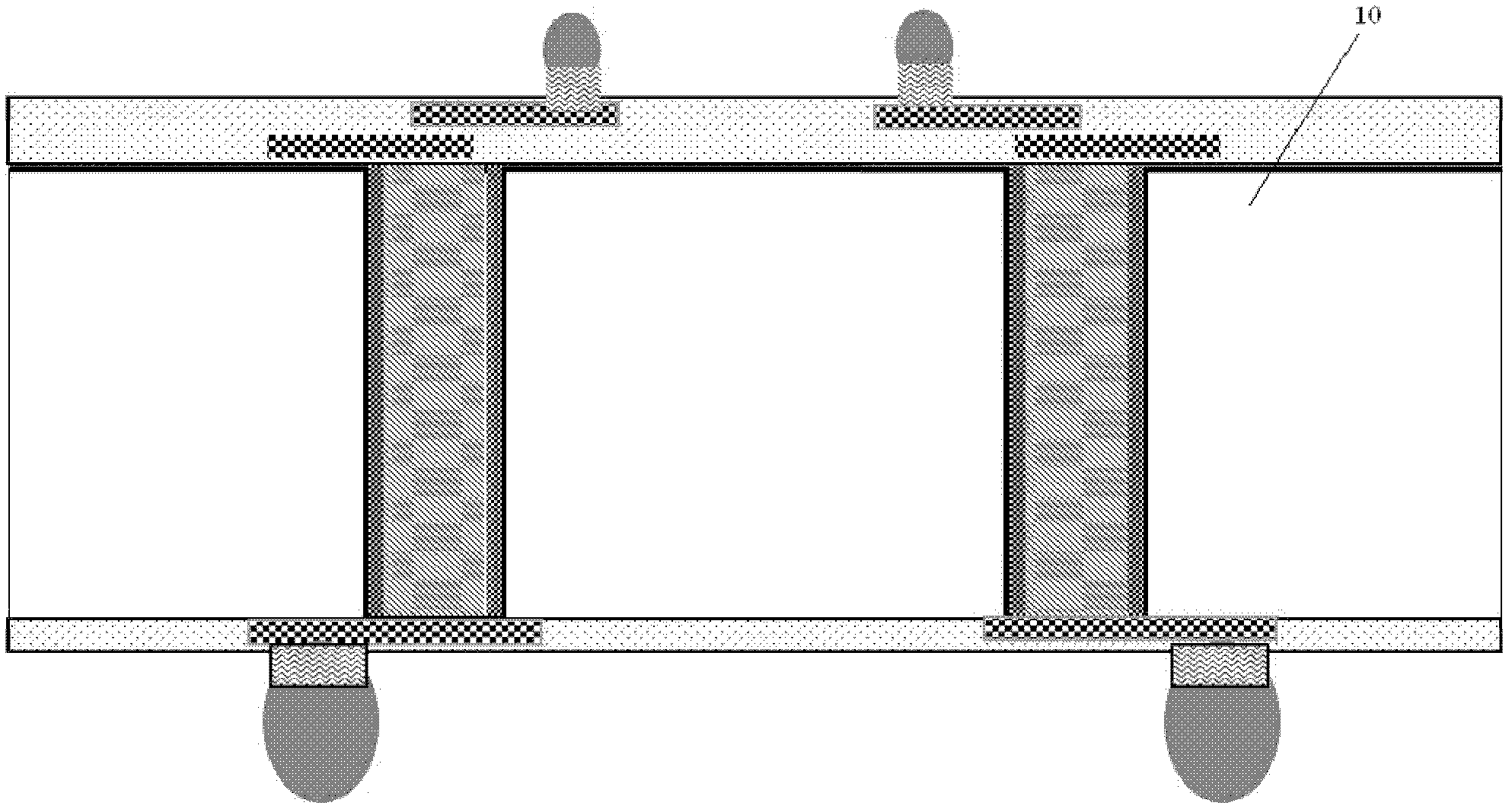
[0044] like figure 1 , figure 2 , Figure 9 and Figure 10 As shown: the vertical interconnection structure in the present invention includes a substrate 10, and the material of the substrate 10 is silicon, gallium arsenide, gallium nitride or glass, and at least one vertical through substrate is arranged in the substrate 10 10 through holes 12 . In order to realize interconnect packaging, when the substrate 10 is a conductor or semiconductor material, an insulating layer 20 is grown on the inner wall of the through hole 12, and the insulating layer 20 is SiO 2 , Si x N 1-x one or more of them. The through hole 12 with the insulating layer 20 grown on the inner wall is filled with an intermetallic compound layer 40, an adhesion layer 30 is provided between the intermetallic compound layer 40 and the insulating layer 20, and the intermetallic compound la...


PUM


Abstract

The invention relates to an intermetallic compound filled vertical through-hole interconnecting structure for three-dimensional package and a preparation method thereof. The vertical through-hole interconnecting structure comprises a substrate, wherein at least one through hole which vertically penetrates through the substrate is formed in the substrate; an insulating layer grows on the inner wall of the through hole; an intermetallic compound layer is filled in the through hole of the grown insulating layer; and an adhesion layer is arranged between the intermetallic compound layer and the insulating layer. At least one through hole which vertically penetrates through the substrate is formed in the substrate; the insulating layer grows on the inner wall of the through hole; the intermetallic compound layer is filled in the through hole; the adhesion layer is arranged between the intermetallic compound layer and the insulating layer; by the intermetallic compound layer, electric connection required in three-dimensional stacking can be finished, the vertical through-hole interconnecting structure is convenient to form and manufacture, and process complexity and manufacturing cost are reduced; and therefore, the vertical interconnecting structure can be manufactured on an integrated circuit, an adapter plate can be manufactured on a passive substrate, the yield is improved, and the vertical through-hole interconnecting structure is safe and reliable.

Description

technical field [0001] The invention relates to a vertical interconnection structure and a preparation method, in particular to a vertical through-hole interconnection structure and preparation method filled with intermetallic compounds for three-dimensional packaging, and belongs to the technical field of three-dimensional integration of microelectronic packaging. Background technique [0002] System-in-Package (SiP) is one of the key technologies of microelectronics, which meets the requirements of high-frequency, high-speed, multi-functional, high-performance, small size and high reliability of electronic devices, and is the direction of electronic technology development. As the feature size of integrated circuits reaches the nanometer level, transistors are developing towards higher density and higher clock frequency, packaging is also developing towards higher density, and integrated circuit products are also developing from two-dimensional to three-dimensional. [0003...

Claims


Application Information

Patent Timeline
Patent Type & Authority Applications(China)
IPC IPC(8): H01L23/522H01L21/768
CPCH01L21/28H01L2224/1403H01L2924/1033H01L2224/13009H01L2224/02377H01L2224/02379H01L2224/05568H01L2224/02372H01L2224/05569H01L2224/14181H01L24/13H01L23/49827H01L2924/14H01L2225/06541H01L2924/01327H01L21/76898H01L2924/00013H01L2224/06181H01L2924/10329H01L2224/0401H01L2224/16145H01L2924/10253H01L23/481H01L2224/02381H01L2225/06548H01L2924/00014H01L2924/00H01L2224/13099H01L2224/05099H01L2224/05599H01L2224/05552
Inventor 于大全
Owner NAT CENT FOR ADVANCED PACKAGING
Why Eureka
Try Eureka