
Novel silicon carbide Schottky diode

A Schottky diode and silicon carbide technology, applied in the field of diodes, can solve problems such as application limitations and large on-resistance, and achieve the effects of improving performance, reducing on-resistance, and increasing reverse blocking voltage

Active Publication Date: 2015-06-17
SEMICON MFG ELECTRONICS (SHAOXING) CORP
View PDF4 Cites 0 Cited by
  • Summary
  • Abstract
  • Description
  • Claims
  • Application Information

AI Technical Summary

Problems solved by technology

[0003] However, the on-resistance of SBD increases rapidly with the increase of its blocking voltage (the specific on-resistance is proportional to the 2.5th power of the blocking voltage), and in higher-voltage SBD devices, its on-resistance will be quite large
As the requirements for blocking voltage become higher and higher, the application of existing structures is significantly limited

Method used


Image

  • Novel silicon carbide Schottky diode

Examples


Embodiment

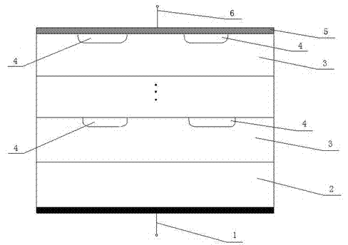
[0012] New SiC Schottky diodes such as figure 1 As shown, it includes SiC substrate 2, the lower end of SiC substrate 2 is connected with cathode 1, the upper end of SiC substrate 2 is connected with SiC epitaxial layer 3, and the upper end of SiC epitaxial layer 3 is connected with Schottky barrier contact metal layer 5. An anode 6 is provided on the base barrier contact metal layer 5, and there are at least two SiC epitaxial layers 3 which are sequentially stacked, the lowermost SiC epitaxial layer 3 is connected to the cathode 1, and the uppermost SiC epitaxial layer 3 is connected to the The Tet-base barrier contact metal layer 5 is connected, and each SiC epitaxial layer 3 forms two p-regions 4 on the surface of the SiC epitaxial layer 3 by P-type ion implantation. The P regions 4 of the respective SiC epitaxial layers 3 do not necessarily have to be aligned with each other.

[0013] When the present invention is working, the forward current enters the Schottky barrier c...


PUM


Abstract

The invention relates to a semiconductor device, and discloses a novel silicon carbide Schottky diode that is applied to high voltage and high frequency systems, such as high power rectification, switching power supply, frequency converter and the like. The novel silicon carbide Schottky diode comprises a SiC substrate (2), wherein the lower end of the SiC substrate (2) is connected with a cathode (1) and the upper end thereof is connected with a SiC epitaxial layer (3). The upper end of the SiC epitaxial layer (3) is connected with a Schottky barrier contact metal layer (5) which is provided with an anode (6). At least two SiC epitaxial layers (3) are arranged and stacked orderly. The lowermost SiC epitaxial layer (3) is connected with the cathode (1) while the uppermost SiC epitaxial layer (3) is connected with the Schottky barrier contact metal layer (5). A P area (4) is arranged on the upper surface of the SiC epitaxial layer (3). The invention improves the reverse blocking voltage of SBD and reduces the conductive resistance of the device by increasing the number of the SiC epitaxial layers so that the conductive loss of the Schottky barrier diode is smaller.

Description

technical field [0001] The invention relates to a semiconductor device, in particular to a diode used in high-voltage and high-frequency systems such as high-power rectification, switching power supply, frequency converter and other devices. Background technique [0002] Schottky barrier diodes (SBDs) are power diodes made using the non-linear characteristics of the potential barrier formed by the contact between the metal and the semiconductor surface. SBD has no additional carrier injection and storage during the conduction process, so there is basically no reverse recovery current, and its turn-off process is very fast, and the switching loss is very small. [0003] However, the on-resistance of SBD increases rapidly with the increase of its blocking voltage (the specific on-resistance is proportional to the 2.5th power of the blocking voltage), and in higher-voltage SBD devices, its on-resistance will be quite large. As the requirements for blocking voltage become highe...

Claims


Application Information

Patent Timeline
Patent Type & Authority Patents(China)
IPC IPC(8): H01L29/872H01L29/06
Inventor 盛况郭清邓永辉崔京京周伟成
Owner SEMICON MFG ELECTRONICS (SHAOXING) CORP
Learn More