
Small-size resistive random access memory and preparation method of small-size resistive random access memory

A technology of resistive variable memory and resistive variable layer, applied in the direction of electrical components, etc., can solve the problems of device resistance distribution, voltage distribution fluctuation, etc., and achieve the effects of high controllability, reduced area, and simple preparation method

Inactive Publication Date: 2012-07-11
PEKING UNIV
View PDF5 Cites 7 Cited by
  • Summary
  • Abstract
  • Description
  • Claims
  • Application Information

AI Technical Summary

Problems solved by technology

However, there are still some problems in RRAM at present, such as large fluctuations in the resistance distribution and voltage distribution of the device, so it is necessary to adopt a new process or a new structure to optimize the performance of the device and suppress the fluctuation of device parameters

Method used


Image

  • Small-size resistive random access memory and preparation method of small-size resistive random access memory
  • Small-size resistive random access memory and preparation method of small-size resistive random access memory

Examples


Embodiment Construction

[0022] The present invention will be further described below through specific embodiments in conjunction with the accompanying drawings. Although this description describes the present invention in detail through specific embodiments, those skilled in the art should understand that the implementation of the present invention is not limited to the scope of description of the embodiments, and the present invention can be modified without departing from the essence and spirit of the present invention. Various modifications and substitutions are made.

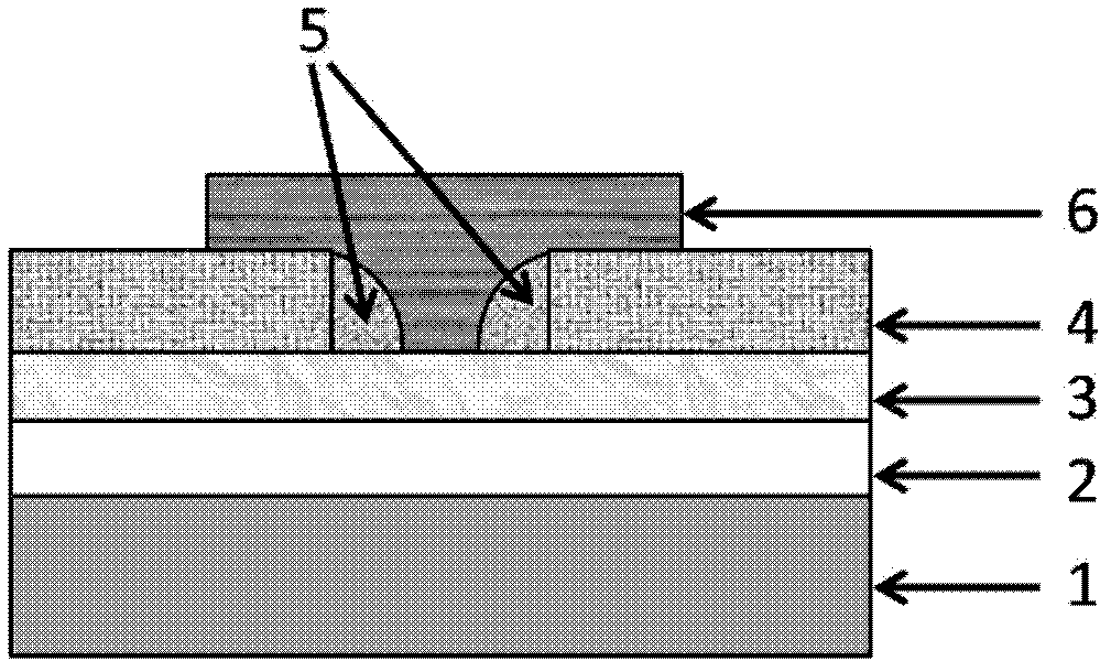
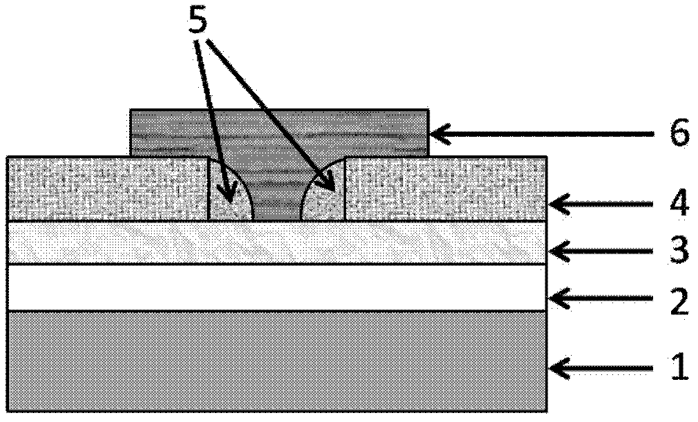
[0023] In this embodiment, the resistive memory such as figure 1 As shown, it includes a substrate 1 (Si), a lower electrode 2 (W or Pt) on the substrate 1, a resistive switch layer 3 (TaO x ), the isolation layer 4 on the resistive switch layer 3 (SiO 2 or SiN, the thickness is less than 50nm), the side walls 5 on both sides of the isolation layer 4 (SiO 2 or SiN), upper electrode 6 (TiN or TaN or Ti or Pt, thickness greater th...


PUM


Abstract

The invention discloses a resistive random access memory structure and a preparation method of the small-size resistive random access memory, belonging to the technical field of CMOS (Complementary Metal Oxide Semiconductors) ultra large scale integrated circuits (ULSI). The resistive random access memory comprises a substrate; a lower electrode is arranged on the substrate; a resistive layer is arranged on an upper electrode; and an isolation layer and the upper electrode are arranged on the resistive layer, wherein the isolation layer is provided with a side wall. In the invention, the resistive change area of the resistive random access memory are effectively controlled in a way that the area of the upper electrode of the resistive random access memory is reduced, so that the fluctuation of parameters of the resistive random access memory is improved.

Description

technical field [0001] The invention relates to a small-size resistive variable memory structure and a preparation method, belonging to the technical field of CMOS ultra-large-scale integrated circuits (ULSI). Background technique [0002] With the development of electronic products, the requirements for storage devices with high performance, high density and high reliability are increasing. In order to meet the needs, the technology nodes of microelectronics are constantly advancing, so that the FLASH technology based on the traditional floating gate structure is encountering serious technical challenges, and its scaled-down technology will eventually be limited by physical limits and cannot continue to advance. In order to solve this problem, a new generation of new non-volatile memory concept - resistive memory RRAM was born. RRAM is completely based on a new storage concept, which is completely different from the traditional concept of flash memory based on threshold vo...

Claims


Application Information

Patent Timeline
Patent Type & Authority Applications(China)
IPC IPC(8): H01L45/00
Inventor 张丽杰黄如
Owner PEKING UNIV
Learn More