
Simple preparation method for metallographic phase sample of silicon wafer

A technology for metallographic sample preparation and silicon wafers, which is applied in semiconductor and photovoltaic production technology and research fields, can solve the problems of inability to take out thin samples completely, long curing time, warping of silicon wafers, etc., to achieve all-round observation and implementation cost The effect of low cost and simple process

Inactive Publication Date: 2012-07-18
SUZHOU XIEXIN INDAL APPL INST
View PDF0 Cites 7 Cited by
  • Summary
  • Abstract
  • Description
  • Claims
  • Application Information

AI Technical Summary

Problems solved by technology

[0003] The technical problem to be solved by the present invention is to provide a simple method for preparing metallographic samples of silicon wafers, which can effectively solve the warping and breaking of silicon wafers caused by the rapid shrinkage of hot and cold mounting methods, and the curing time is long , high cost and other problems, and also solve the problem that the samples prepared by the hot mounting method and the cold mounting method cannot be completely taken out for a series of follow-up experiments

Method used


Image

  • Simple preparation method for metallographic phase sample of silicon wafer
  • Simple preparation method for metallographic phase sample of silicon wafer
  • Simple preparation method for metallographic phase sample of silicon wafer

Examples


Embodiment 1

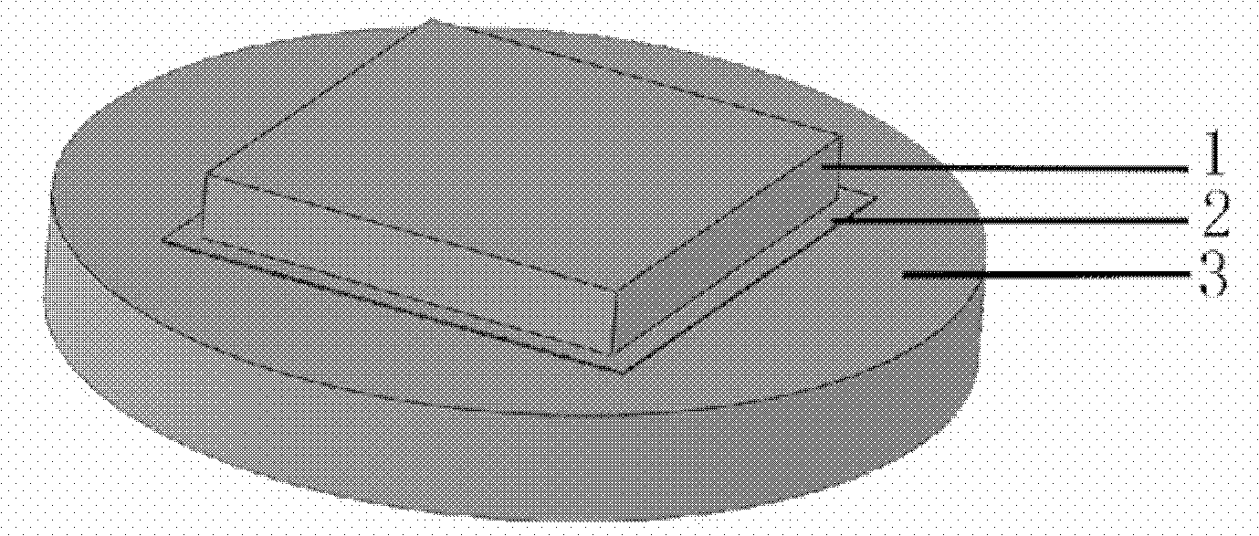
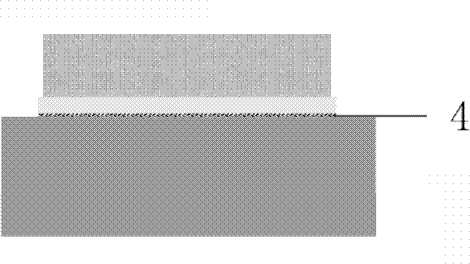
[0026] A kind of simple and easy preparation method of silicon chip metallographic sample, it comprises the steps:

[0027] (1) Select a flat stainless steel, hard alloy or ceramic cylinder (diameter 40mm, height 10mm) as the carrier plate of the silicon wafer;

[0028] (2) Put the solid hot melt adhesive on the surface of the carrier board, the dosage is 0.3 ~ 0.5g, the dosage is enough to adhere to the silicon wafer, and the carrier board is heated until the hot melt adhesive melts into a liquid thin layer (according to the hot melt adhesive characteristics, generally heated to 70 ~ 100 ℃, about 2 minutes to melt);

[0029] (3) After the hot melt adhesive is melted, place the silicon wafer (thickness below 250 μm) flat on the upper surface of the carrier and cover it on the hot melt adhesive, and use another flat pressing block (generally weighing 50 to 100 g) to evenly Apply pressure on the silicon wafer to make the thin silicon wafer closely adhere to the surface of the c...


PUM

PropertyMeasurementUnit
Thicknessaaaaaaaaaa

Abstract

The invention disclosers a simple preparation method for a metallographic phase sample of a silicon wafer. A flat cylinder is used as a carrier plate of the silicon wafer, and the method comprises the following steps of: placing a hot melt adhesive on the carrier plate, and heating the carrier plate until the hot melt adhesive is molten; flatly placing the silicon wafer in the middle of the carrier plate and covering on the hot melt adhesive, and applying force to the silicon wafer by using the other flat pressing block; cooling the carrier plate to room temperature to ensure that the hot melt adhesive is cured; polishing the prepared sample; after polishing, heating the carrier plate again to ensure that the cured hot melt adhesive is molten, allowing the silicon wafer to fall off and taking down the silicon wafer; and washing the silicon wafer to finish the metallographic phase sampling of an ultra thin silicon wafer. The process is simple, and is convenient to operate, and low in implement cost; and the prepared thin silicon wafer sample is not warped or crushed, and is stable during polishing; the key point is that after processing, the silicon wafer can be conveniently taken out, the omnibearing observation of the microstructure of the ultra thin silicon wafer can be realized, the specific area can be selected conveniently for component or structure analysis, and in-situ multi-angle and multi-means representation and detection of the specific area of the silicon wafer can be performed.

Description

technical field [0001] The patent of the invention relates to the field of semiconductor and photovoltaic production technology and research, in particular to a simple metallographic sample preparation method based on ultra-thin and fragile silicon wafer materials. Background technique [0002] At present, the thickness of silicon wafers used for solar grades is generally less than 250 μm, and they are brittle and easy to break. When making samples for microscopes and scanning electron microscopes, they must be mounted. Traditional metallographic sample preparation mainly includes hot-mounting and cold-mounting methods. For ultra-thin silicon wafers, the heating and pressurization process of the hot-mounting method can easily cause the sample to break, while the cold-mounting method takes a long time to solidify and is expensive. Shrinkage of the cold mounting agent can easily cause excessive internal stress of the silicon wafer, warping and breaking of the thin silicon wafe...

Claims


Application Information

Patent Timeline
IPC IPC(8): G01N1/28
Inventor 宫龙飞王风振
Owner SUZHOU XIEXIN INDAL APPL INST
Learn More