Storage unit and single-end low-swing bit line writing circuit

A writing circuit, single-ended technology, applied in the field of writing circuits, can solve the problems of high power consumption and inapplicability

Inactive Publication Date: 2012-07-18
INST OF ACOUSTICS CHINESE ACAD OF SCI
View PDF4 Cites 11 Cited by
  • Summary
  • Abstract
  • Description
  • Claims
  • Application Information

AI Technical Summary

Problems solved by technology

Disadvantages of the existing technology: the bit line is rail-to-rail, so the power consumption required to complete the write operation is relatively large
The disadvantages of various write operations

Method used


Image

  • Storage unit and single-end low-swing bit line writing circuit
  • Storage unit and single-end low-swing bit line writing circuit
  • Storage unit and single-end low-swing bit line writing circuit

Examples


Embodiment Construction

[0077] The present invention will be further described below in conjunction with the accompanying drawings and embodiments.

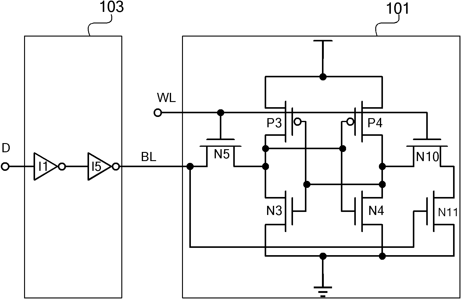
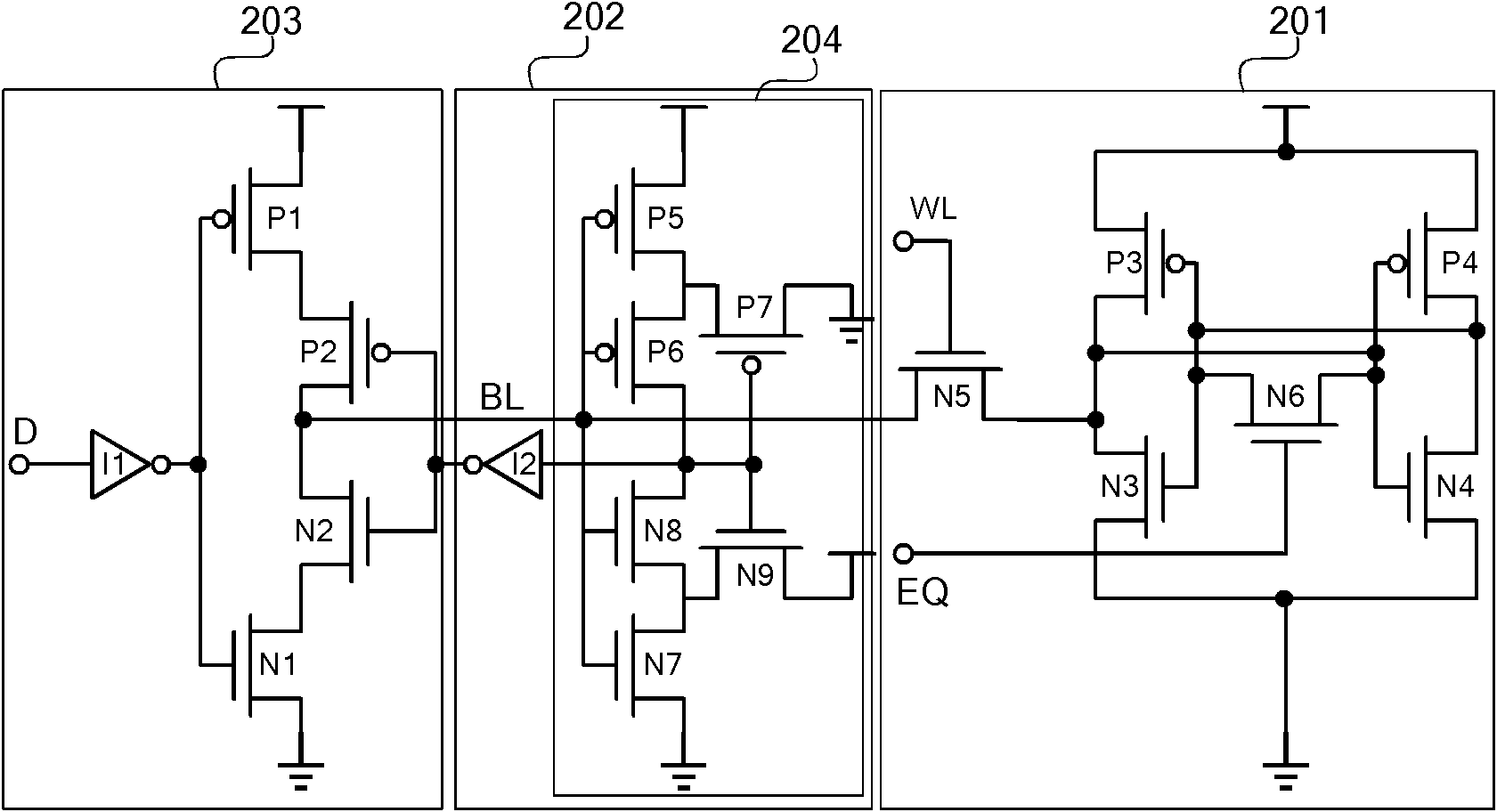
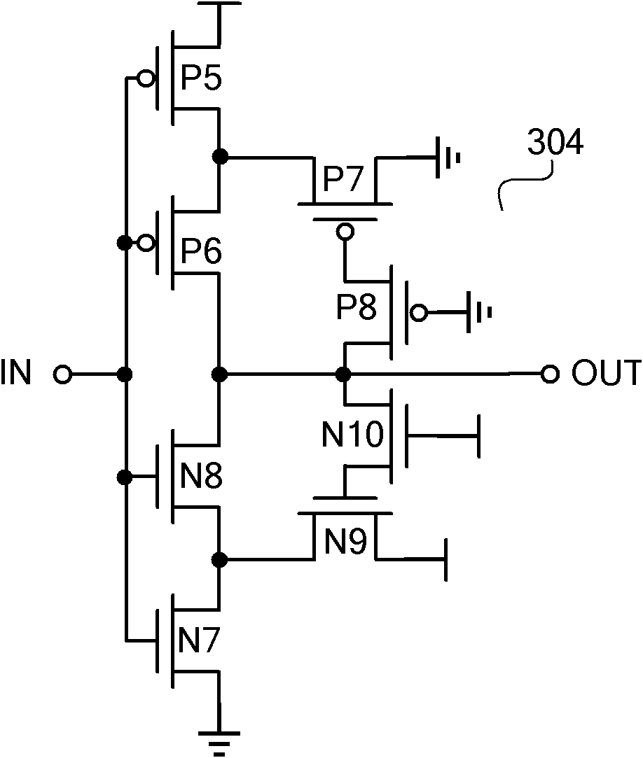
[0078] figure 2 It is a memory unit and a single-end low-swing bit line writing circuit diagram of the present invention. Such as figure 2 As shown, I1 and I2 are inverters, P1, P2, P3, P4, P5, P6, and P7 are PMOS transistors, and N1, N2, N3, N4, N5, N6, N7, N8, and N9 are NMOS transistors.

[0079]The gate of P1 and the gate of N1 are connected to the output terminal of I1; the source of P1 is connected to the power supply voltage; the drain of P1 is connected to the source of P2; the gate of P2 is connected to the output terminal of I2 and the gate of N2 ; The drain of P2, the grid of P5, the grid of P6, the grid of N7, the grid of N8 and the drain of N2 are connected with the bit line signal BL; the drain of N1 is connected with the source of N2; The source is grounded; the gate of P3, the drain of P4, the gate of N3 and the drain of N4 are conn...


PUM


Abstract

The invention relates to a storage structure and a single-end low-swing bit line writing circuit. The circuit comprises at least one storage unit and a driving circuit, wherein the driving circuit comprises a first phase inverter (I1), and the input end of the first phase inverter (I1) is used for writing data (D). The circuit is characterized in that the driving circuit also comprises a first P-channel metal oxide semiconductor (PMOS) transistor (P1), a second PMOS transistor (P2), a first N-channel metal oxide semiconductor (NMOS) transistor (N1) and a second NMOS transistor (N2), the writing circuit also comprises a feedback control circuit, the storage unit comprises a third PMOS transistor (P3), a fourth PMOS transistor (P4), a third NMOS transistor (N3), a fourth NMOS transistor (N4), a fifth NMOS transistor (N5) and a sixth NOMS transistor (N6). The assistance of additional reference voltage or power supply voltage is not needed for realizing the low-swing technology, and in addition, the single-end single-swing writing is supported through the improved storage unit.

Description

technical field [0001] The invention relates to a writing circuit for on-chip memory, in particular to a storage unit and a single-end low swing bit line writing circuit. Background technique [0002] In the design of multi-port static memory or register file, a single-ended structure is generally used to achieve high-density design. figure 1 Write circuit diagrams for state-of-the-art memory cells and single-ended bit lines, such as figure 1 shown. The existing circuit includes: a driving circuit 103 and a storage unit 101 . D represents buffered or latched data, BL (bitline) represents a bit line, WL (word line) represents a word line, and I1 and I5 are two inverters. Generally, several memory cells are connected to the bit line BL, but the word line WL signals of these memory cells are respectively connected to different word lines. [0003] When the data D is to be written into a memory cell through the bit line, the data D first drives the bit line BL through the in...

Claims


Application Information

Patent Timeline
IPC IPC(8): G11C11/416
Inventor 王东辉闫浩洪缨侯朝焕
Owner INST OF ACOUSTICS CHINESE ACAD OF SCI
Why Eureka
Try Eureka