Chip back side drape tin eutectic technology and loading method thereof

A chip and tin coating technology, which is applied to the tin coating eutectic process on the back of the chip and the field of chip loading, can solve the problems of chip rotation or twisting, chip size requirements, scrapping and other problems, so as to improve the quality of chip loading and reliable packaging. The effect of sexual enhancement and avoidance of delamination

Inactive Publication Date: 2012-07-18
CHANGJIANG ELECTRONICS TECH CHUZHOU
View PDF2 Cites 3 Cited by
  • Summary
  • Abstract
  • Description
  • Claims
  • Application Information

AI Technical Summary

Problems solved by technology

Lead-tin soldering chip mounting can combine the advantages of eutectic chip mounting and conductive adhesive chip mounting. The main defect of this chip mounting method is the requirement for chip size. If the chip size is too small, it will The chip will rotate or twist, resulting in defective and scrapped

Method used


Image

  • Chip back side drape tin eutectic technology and loading method thereof
  • Chip back side drape tin eutectic technology and loading method thereof

Examples


Embodiment Construction

[0028] A kind of tin eutectic process and chip loading method of the present invention, it comprises the following process steps:

[0029] Step 1. Use the existing mature technology to process the back of the chip with silver or gold;

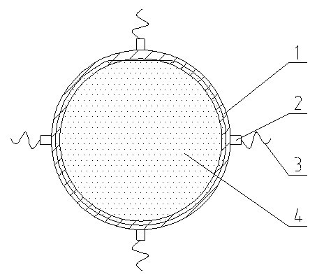
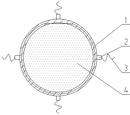
[0030] Step 2. Place the chip with back silver or back gold treatment on the tooling fixture (such as figure 1 As shown), the jig and the chip are electroplated with tin or tin alloy. At this time, the back silver or back gold of the chip will be plated with a layer of tin or tin alloy, and the thickness and speed of the coating can be controlled;

[0031] The tooling fixture includes a fixture body 1, the fixture body 1 is annular, and a plurality of electroplating pins 2 are evenly distributed on the outer edge of the annular fixture body 1. During electroplating, the electroplating pins 2 is connected with wires, and the chip 4 is placed on the fixture body 1 with the front facing up.

[0032] The back silver or gold back surface of the ch...


PUM


Abstract

The invention relates to a chip back side drape tin eutectic technology and a loading method thereof. The method comprises the following steps: step (1), carrying out backside silver or backside gold processing on a chip back side; step (2), carrying out tinning or tin alloy work on a backside silver surface or a backside gold surface of a chip which is subjected to the backside silver or backside gold processing in the step (1); step (3), cutting the chip whose backside silver surface or backside gold surface is subjected to the tinning or tin alloy work in the step (2); step (4), employing eutectic technology to install the chip which is cut in the step (3) to a basic island to complete loading. According to the chip back side drape tin eutectic technology and the loading method, there is no requirement to chip dimension, after the chip back side is coated with a layer of tin or tin alloy, since the thickness of the tin or tin alloy can be controlled, the thickness of the tin or tin alloy can effectively absorb different stresses between the chip and the basic island, and lamination and rupture problems of a traditional eutectic chip are solved.

Description

technical field [0001] The invention relates to a tin eutectic process for coating the back of a chip and a chip loading method thereof, and belongs to the technical field of semiconductor packaging. Background technique [0002] In the field of medium and high-power semiconductor packaging, there are mainly three traditional chip mounting technologies: one is eutectic chip mounting, the other is conductive adhesive chip mounting, and the third is lead-tin soldering chip mounting, and lead-tin soldering chip mounting It can be subdivided into lead-tin wire mounting and lead-tin glue mounting, but at present, these several mounting methods have their own defects: [0003] 1. Eutectic loading [0004] For eutectic chip mounting, a layer of gold or gold-arsenic alloy or silver alloy needs to be plated on the back of the chip, and then a layer of silver is generally plated on the base island chip mounting position, and then eutectic chip mounting can be performed. During eutec...

Claims


Application Information

Patent Timeline
Patent Type & Authority Applications(China)
IPC IPC(8): H01L21/48H01L21/60
Inventor 谢洁人王新潮俞斌吴昊
Owner CHANGJIANG ELECTRONICS TECH CHUZHOU
Why Eureka
Try Eureka