

Manufacturing method of semiconductor device
A manufacturing method and semiconductor technology, applied in the direction of semiconductor/solid-state device manufacturing, semiconductor devices, manufacturing tools, etc., can solve the problems of unavoidable semiconductor device manufacturing cost, increase, design constraints, etc., and achieve the suppression of voids and poor connections. Effect
- Summary
- Abstract
- Description
- Claims
- Application Information
AI Technical Summary
Problems solved by technology
Method used
Image

Examples
no. 1 Embodiment approach
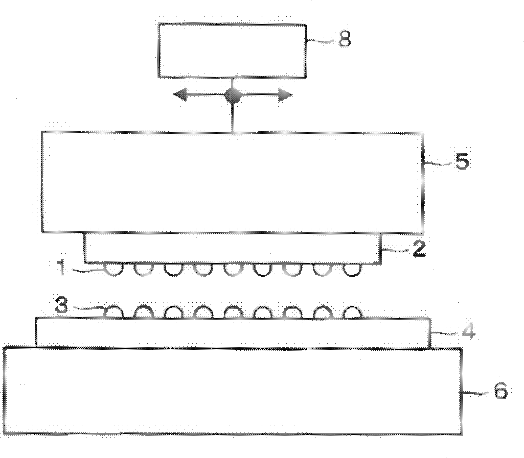
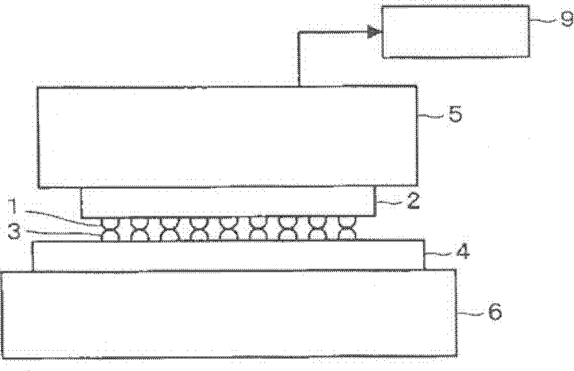
[0026] Figure 1 ~ Figure 4 It is a figure showing the manufacturing process of the semiconductor device of 1st Embodiment. The first embodiment is a method of manufacturing a semiconductor device using flip-chip connection without using flux. Such as figure 1 As shown, a first substrate 2 having first solder bumps 1 and a second substrate 4 having second solder bumps 3 are prepared. The first substrate 2 is held, for example, by suction on the tool 5 . The second substrate 4 is arranged on a stage 6 . from figure 1 Alignment procedure shown to image 3 The temporary connection process shown is implemented using a flip-chip bonder equipped with an alignment mechanism, a heating mechanism, a height restriction mechanism, and the like.
[0027] The first substrate 2 and the second substrate 4 are, for example, semiconductor chips (silicon (Si) chips, etc.) or interposer chips (silicon (Si) interposers, etc.). The combination of the first substrate 2 and the second substra...
no. 2 Embodiment approach
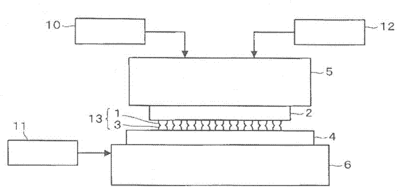
[0043] Figure 6 ~ Figure 9 It is a figure which shows the manufacturing process of the semiconductor device of 2nd Embodiment. In the manufacturing process of the semiconductor device according to the second embodiment, first, the first substrate 2 having the first solder bumps 1 and the second substrate having the second solder bumps 3 are prepared in the same manner as in the first embodiment. 4, such as Image 6 As shown, the first solder bump 1 and the second solder bump 3 are aligned. Specific examples of the substrates 2 and 4 , constituent materials of the solder bumps 1 and 3 , alignment method of the solder bumps 1 and 3 , and the like are the same as those of the first embodiment. Additionally, from Image 6 Alignment procedure shown to Figure 8 The temporary connection step shown is implemented using a flip-chip bonder equipped with an alignment mechanism, a pressurization mechanism, a heating mechanism, an ultrasonic generating mechanism, and the like.
[00...
Embodiment 1
[0052] First, a first semiconductor chip on which solder bumps composed of Sn-0.7 mass % Cu are formed on electrode terminals by electroplating, and a second semiconductor chip on the connected side mounted with the first solder bumps are prepared. Solder bumps composed of Sn-0.7% by mass Cu are formed on the electrode terminals of the second semiconductor chip in the same manner as the first semiconductor chip 1 . The electrode terminals of the first semiconductor chip and the electrode terminals of the second semiconductor chip are arranged at corresponding predetermined positions so as to be connectable to each other. The number of terminals is about 2000, the height of the solder bump is 20 μm, and the minimum distance between adjacent terminals is 60 μm. No flux was used.
[0053] For these semiconductor chips, the first semiconductor chip held on the tool and the second semiconductor chip held on the stage are connected by a flip chip bonder equipped with an alignment m...
PUM
| Property | Measurement | Unit |
|---|---|---|
| height | aaaaa | aaaaa |
Abstract
Description
Claims
Application Information