Solar cell component structure

A solar cell and component technology, applied in electrical components, circuits, photovoltaic power generation, etc., can solve problems such as deepening health, human health hazards, environmental pollution, etc., and achieve the effect of reducing waste liquid and avoiding cadmium pollution of the environment.

Inactive Publication Date: 2012-07-18
PVNEXT CORP
View PDF3 Cites 4 Cited by
  • Summary
  • Abstract
  • Description
  • Claims
  • Application Information

AI Technical Summary

Problems solved by technology

[0004] If the buffer layer contains cadmium sulfide (CdS), because cadmium is toxic, it will cause considerable harm to human health if eaten
Therefore, if there is cadmium in solar cell components, if they are not properly disposed of in the future, it may cause environmental pollution and increase the suspicion of health threats.
[0005] In addition, CdS is generall

Method used


Image

  • Solar cell component structure
  • Solar cell component structure
  • Solar cell component structure

Examples


Embodiment Construction

[0023] The making and use of the presently preferred embodiments of the present invention are discussed in detail below. However, it should be understood that the present invention provides many applicable devices, which can be implemented in a variety of specific situations. The specific examples discussed only illustrate specific ways to make and use the invention, and do not limit the scope of the invention.

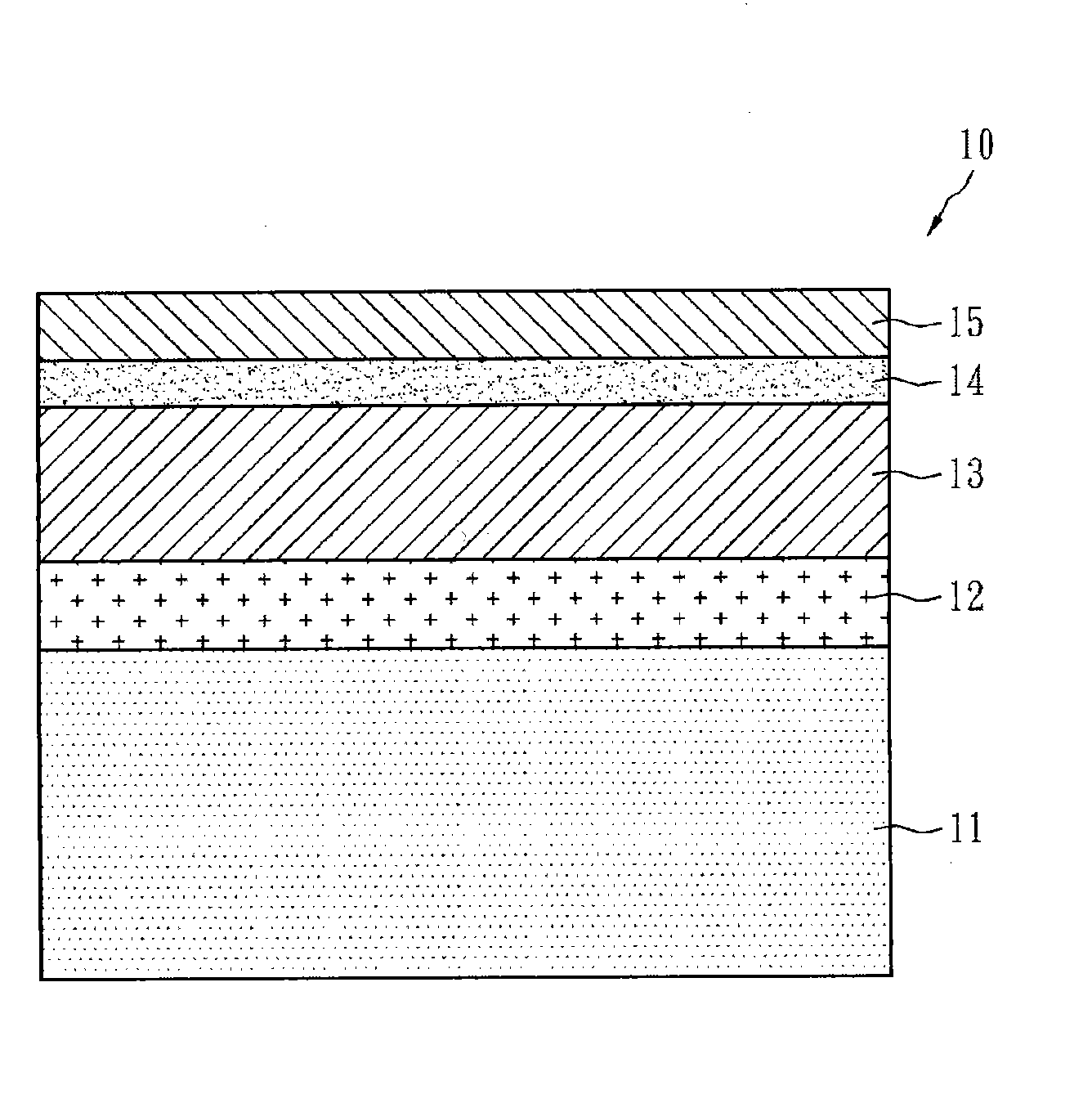
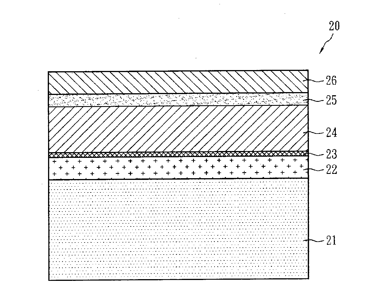
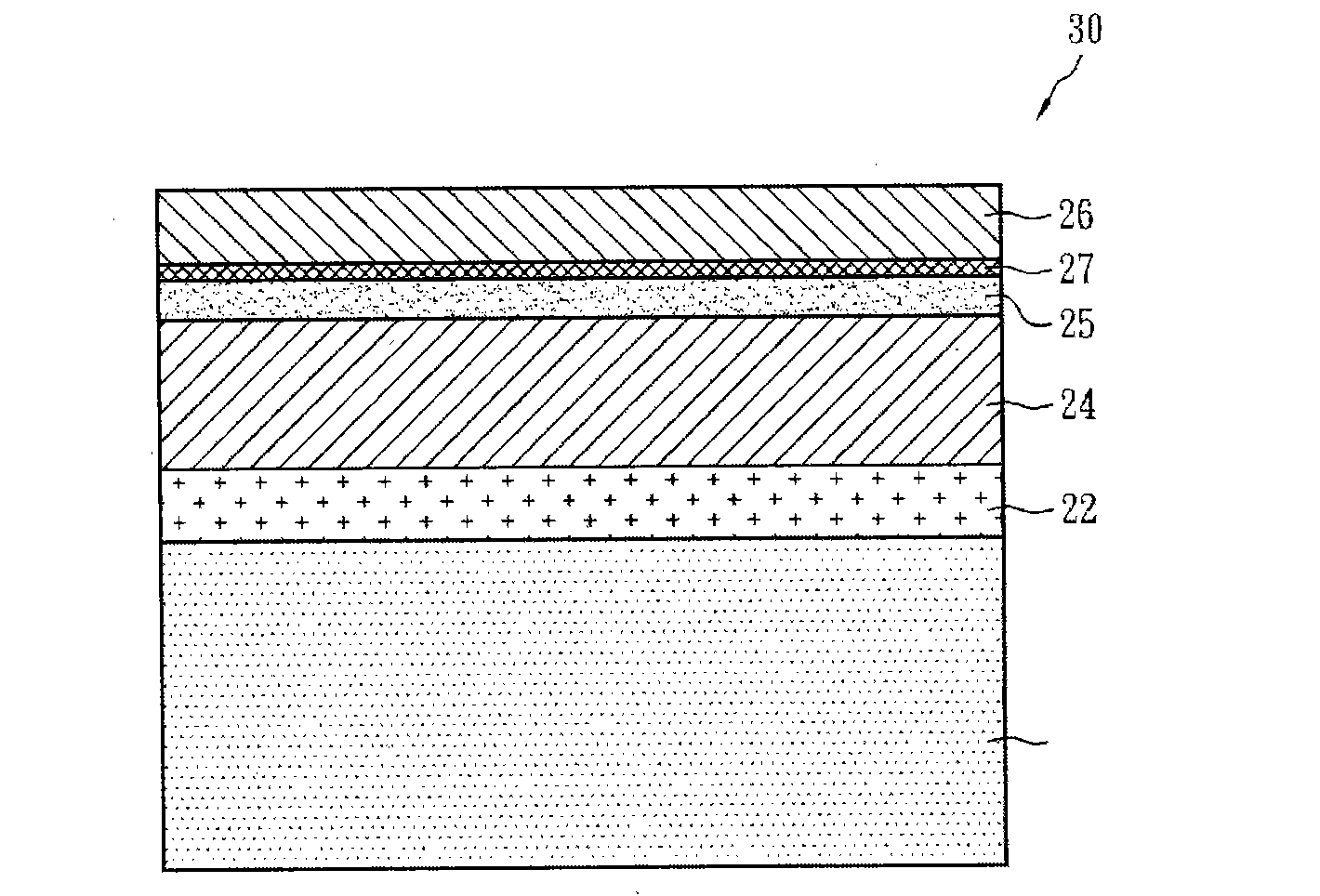
[0024] figure 2 The structure of the solar cell element according to the first embodiment of the present invention is shown. The solar device structure 20 is a laminated structure, which includes a substrate 21, a metal layer 22, a high-resistance film layer 23, a p-type semiconductor layer 24, an n-type semiconductor layer 25 and a transparent conductive layer 26. The substrate 21 is generally a glass substrate, and it may also be a metal plate or metal foil such as polyimide, stainless steel, molybdenum, copper, titanium, and aluminum. The above-mentioned substrate ...


PUM

PropertyMeasurementUnit
Thicknessaaaaaaaaaa
Thicknessaaaaaaaaaa

Abstract

The invention discloses a solar cell component structure comprising a substrate, a metal layer, a p-type semiconductor layer, an n-type semiconductor layer, a transparent conductive layer and a high resistance film layer, wherein the metal layer is formed on the surface of the substrate; the p-type semiconductor layer is formed on the metal layer and comprises copper indium gallium selenium sulfur (CIGSS), copper indium gallium selenium (CIGS), copper indium sulfur (CIS), copper indium selenium (CIS) or a compound material containing two or two more of copper, selenium or sulfur; the n-type semiconductor layer has the photocatalyst characteristics (such as improvement of carrier mobility by using irradiation), is formed on the surface of the p-type semiconductor layer and forms a p-n joint surface together with the p-type semiconductor layer; the transparent conductive layer is formed on the n-type semiconductor layer; and the high resistance film layer is formed between the metal layer and the transparent conductive layer.

Description

Technical field [0001] The present invention relates to a solar cell structure, in particular to a thin-film solar cell structure containing four elements of copper indium gallium selenium (CIGS). Background technique [0002] Among the thin-film solar cells, there are two types of photoelectric cell meters of Copper Indium Gallium Diselenide Solar Cells: one containing three elements of copper indium selenium (CIS) and one containing four elements of copper indium gallium selenium (Referred to as CIGS). Because of its high photoelectric efficiency and low material cost, it is favored by many people. The photoelectric efficiency of CIGS photovoltaic cells completed in the laboratory can reach up to about 19%, and as far as the module is concerned, it can reach up to about 13%. [0003] figure 1 A conventional CIGS solar cell structure 10 is disclosed, which is a laminated structure including a substrate 11, a metal layer 12, a CIGS layer 13, a buffer layer 14 and a transparent co...

Claims


Application Information

Patent Timeline
IPC IPC(8): H01L31/04H01L31/0336
CPCY02E10/50
Inventor 章丰帆林信志林信宏谢季桦李宗龙
Owner PVNEXT CORP
Why Eureka
Try Eureka