Light source packaging structure and manufacturing method thereof as well as liquid crystal display

A technology of a packaging structure and a manufacturing method, which are applied in the field of a light source packaging structure and a manufacturing method and a liquid crystal display, can solve the problems of reduced lifespan, burnt yellow, easy cracking and discoloration of epoxy resin, etc., and achieve the effect of reducing the chance of damage

Inactive Publication Date: 2012-07-18
ASDA TECH
View PDF6 Cites 13 Cited by
  • Summary
  • Abstract
  • Description
  • Claims
  • Application Information

AI Technical Summary

Problems solved by technology

Among them, epoxy resin is easy to crack and change color, resulting in reduced lifespan. In addition, the light source emitted by light-emitting diodes (especially blue and white light) contains ultraviolet (Ultraviolet light, UV) bands, which will cause carbonization of epoxy resin and produce burnt yellow. Phenomenon, reducing the light-emitting efficiency of light-emitting diodes
[0003] In view of this, the industry has changed to silicone (silicone) glue instead of epoxy resin as the outer layer of the LED package. However, silicone has high water absorption and low air tightness, and it is easy for water vapor to penetrate into the LED. As a result, the lifespan of the phosphor is reduced and its original effectiveness is quickly lost, so many companies still have to find a more suitable solution to improve the performance of the packaging application of light emitting diodes (light emitting diodes)
[0004] It can be seen that the above-mentioned packaging application technology still has inconvenience and defects, and needs to be further improved, especially the carbonization of epoxy resin and the moisture penetration of silicone
In order to seek a more suitable solution, related fields have tried their best to find a solution, but no applicable method has been developed for a long time

Method used


Image

  • Light source packaging structure and manufacturing method thereof as well as liquid crystal display
  • Light source packaging structure and manufacturing method thereof as well as liquid crystal display
  • Light source packaging structure and manufacturing method thereof as well as liquid crystal display

Examples


no. 4 example

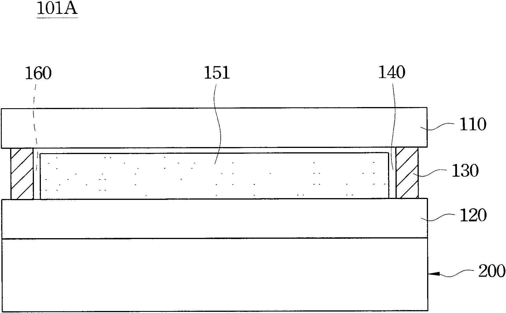
[0156] In this fourth embodiment, the liquid crystal panel 510 includes an upper substrate 511 and a liquid crystal layer 512 . The first substrate 110 of the above-mentioned light source packaging structure 100 is the lower substrate of the liquid crystal panel 510 , which means that the liquid crystal layer 512 is directly sandwiched between the upper substrate 511 of the liquid crystal panel 510 and the first substrate 110 of the light source packaging structure 100 . Therefore, on the one hand, the liquid crystal display 500 of the present invention can save the material cost of a glass substrate, and on the other hand, can reduce the distance of light traveling to the liquid crystal panel 510 .

[0157] see Figure 13A as shown, Figure 13A A schematic side view of a variation of the fourth embodiment of the liquid crystal display 500 combined with the light source packaging structure 100A of the present invention is shown.

[0158] This change is the design of the liqu...


PUM

PropertyMeasurementUnit
thicknessaaaaaaaaaa

Abstract

The invention discloses a light source packaging structure and a manufacturing method thereof as well as a liquid crystal display. The light source packaging structure comprises two overlapped substrates, frame-shaped colloid, a filler layer and a luminescent material, wherein the frame-shaped colloid is positioned in the two substrates and commonly define a vacuum space together with the substrates; the luminescent material is positioned in the vacuum space; and the filler layer has light transparency, is fully filled in the vacuum space and coats the luminescent material. In each embodiment of the invention, the luminescent material is a fluorescent powder layer or a light emitting diode or the coexistence of the fluorescent powder layer and the light emitting diode respectively.

Description

technical field [0001] The present invention relates to a packaging structure, in particular to a light source packaging structure, a manufacturing method thereof, and a liquid crystal display. Background technique [0002] In conventional packaging applications of light emitting diodes, for example, epoxy resin is used as an adhesive material for the outer layer of the packaging of light emitting diodes. Among them, epoxy resin is easy to crack and change color, resulting in reduced lifespan. In addition, the light source emitted by light-emitting diodes (especially blue and white light) contains ultraviolet (Ultraviolet light, UV) bands, which will cause carbonization of epoxy resin and produce burnt yellow. Phenomenon, reducing the light-emitting efficiency of light-emitting diodes. [0003] In view of this, the industry has changed to silicone (silicone) glue instead of epoxy resin as the outer layer of the LED package. However, silicone has high water absorption and lo...

Claims


Application Information

Patent Timeline
Patent Type & Authority Applications(China)
IPC IPC(8): H01L33/48H01L33/54G02F1/13357H01L33/00
CPCH01L2924/0002H01L51/5036H01L33/504G02F1/133621H01L51/5246H01L33/00F21K9/00H01L33/46G02F1/133603H01L25/0753H01L33/48H01L33/501H01L33/507H01L51/5253H01L33/54H01L2924/00
Inventor 林柏廷
Owner ASDA TECH
Why Eureka
Try Eureka