Wave aberration measuring device and method

A measurement device and technology of wave aberration, which is applied in the direction of photolithographic exposure device, test optical performance, microlithography exposure equipment, etc. Real-time performance and the effect of improving the measurement speed

Active Publication Date: 2012-07-25
SHANGHAI MICRO ELECTRONICS EQUIP (GRP) CO LTD
View PDF7 Cites 17 Cited by
  • Summary
  • Abstract
  • Description
  • Claims
  • Application Information

AI Technical Summary

Problems solved by technology

[0005] The technical problem solved by the present invention is that the existing phase-shift shearing method measures the wave aberration of the photolithography device for a long time and cannot meet the technical problem of real-time requirements

Method used


Image

  • Wave aberration measuring device and method
  • Wave aberration measuring device and method
  • Wave aberration measuring device and method

Examples


Embodiment Construction

[0040] Specific embodiments of the present invention will be described in detail below in conjunction with the accompanying drawings.

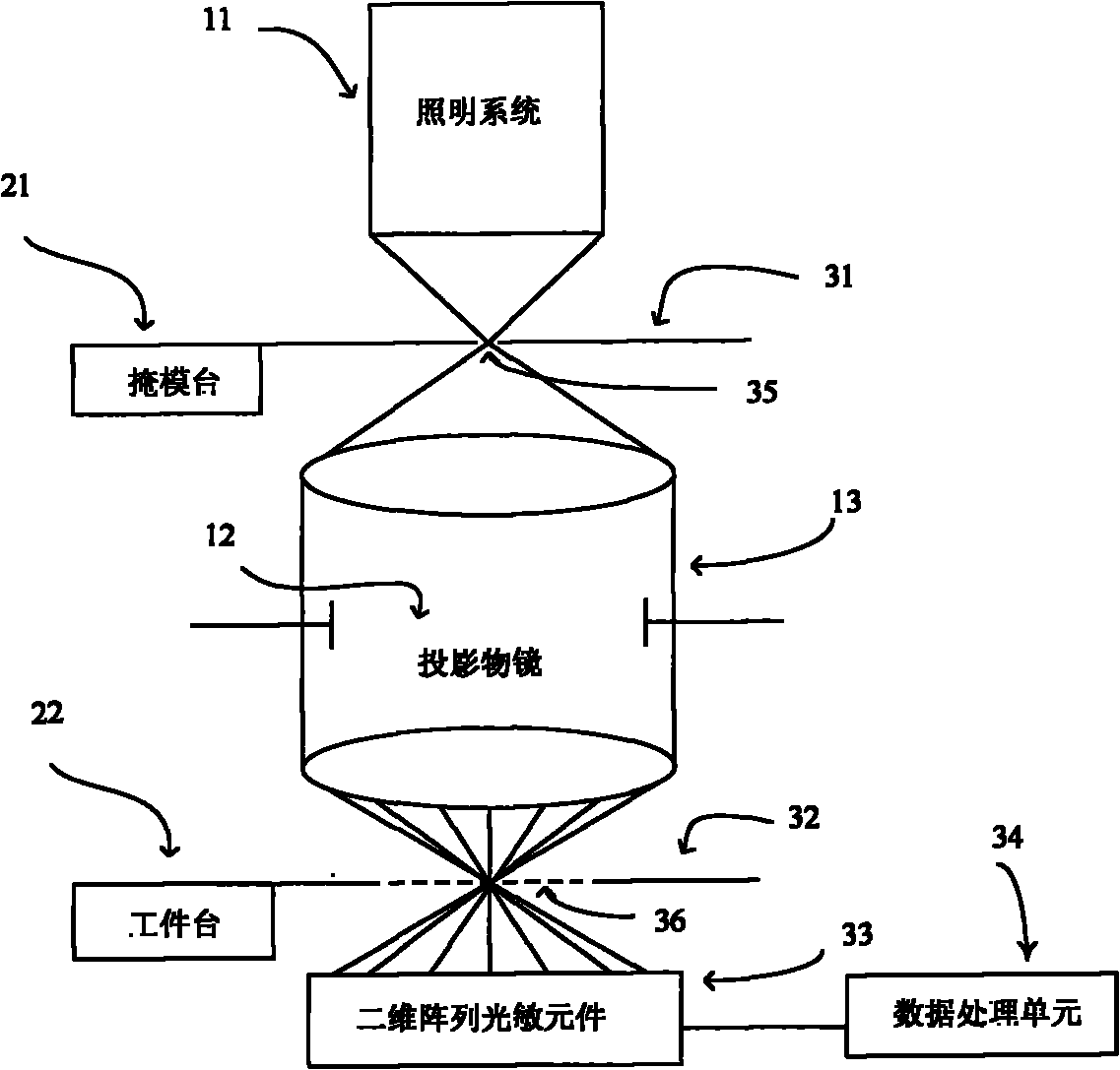
[0041] refer to figure 1 , the wave aberration measuring device of the present invention comprises:

[0042] The lighting system 11 generates lighting light;

[0043] Object surface aperture plate 31, has object surface aperture 35 on it;

[0044] An image plane shearing grating plate 32 having an image plane shearing grating 36 thereon;

[0045] A two-dimensional array photosensitive element 33 and a data processing unit 34 .

[0046] In the embodiment of the above-mentioned wave aberration measuring device, the object plane small hole plate 31 is located under the illumination system 11 of the lithography machine, and the object plane of the projection objective lens 13 is connected with the mask table 21 and can be accompanied by the mask table 21. sports. The object plane aperture plate 31 receives the illumination light from the illu...


PUM


Abstract

The invention relates to a wave aberration measuring device and method. An illumination system produces an illumination beam; an object surface small hole comprises at least two object surface small hole marks, the at least two object surface small hole marks are arranged along a first direction, the object surface small hole marks comprise two object surface small hole sub marks, the two object surface small hole sub marks are arranged along a second direction, the first direction is vertical to the second direction, the grating directions of the two object surface small hole sub marks are respectively an X direction and a Y direction, and the illumination beam irradiates the object surface small hole to form a measuring beam; the measuring beam passes through a projection objective lens and then shoots an image surface shear grating so as to form a shear interference pattern; and a two-dimensional array photosensitive element obtains a plurality of shear interference patterns in the two directions through repeatedly changing the relative positions of the object surface small holes and the shear interference pattern, so as to calculate the wave aberration of the projection objective lens. According to the wave aberration measuring device and method, the wave aberration of multi-view-field points can be measured, so that the parallel measurement on the wave aberration of the multi-view-field points of a photoetching device is realized; and the measuring speed is fast, and the real-time performance is high.

Description

technical field [0001] The invention relates to the field of wave aberration measurement, in particular to a multi-field point wave aberration measurement device and a measurement method for a lithography device. Background technique [0002] One goal of the semiconductor industry is to integrate more electronic components into a single integrated circuit (IC). To achieve this goal, the size of the components must be continuously reduced, that is, the resolution of the lithography projection system must be continuously improved. Objective lens wave aberration is an important factor limiting the resolution of a projection system, and it is an important cause of line width variation. [0003] Although the objective lens has been strictly inspected and optimized during the manufacturing and assembly process to minimize its wave aberration, it is still necessary to perform online wave aberration measurement after the objective lens system is integrated into the lithography mach...

Claims


Application Information

Patent Timeline
Patent Type & Authority Applications(China)
IPC IPC(8): G03F7/20G01M11/02
Inventor 陆海亮王帆
Owner SHANGHAI MICRO ELECTRONICS EQUIP (GRP) CO LTD
Why Eureka
Try Eureka