Three-dimensional circuit on structure member and manufacturing method thereof

A technology of three-dimensional circuit and manufacturing method, which is applied in the directions of printed circuit components, printed circuit secondary processing, conductive pattern formation, etc., can solve the problems of low product yield, high price, and influence of circuit size, etc., to save production costs, Anti-corrosion, non-destructive effect

Active Publication Date: 2015-06-03
苏州同拓光电科技有限公司
View PDF6 Cites 0 Cited by
  • Summary
  • Abstract
  • Description
  • Claims
  • Application Information

AI Technical Summary

Problems solved by technology

Most of these processes are used in the production of flat circuits, among which the silk screen process cannot realize three-dimensional circuits, while the spraying process needs to make complex masking tools with low resolution; the pad printing process has the opportunity to realize some three-dimensional circuits. It is to use the silicone head to absorb the conductive ink in the groove of the concave plate and then press the silicone head to the surface of the structural part, so as to transfer the conductive ink to the pre-selected area on the surface of the workpiece, but because the rubber head is an elastic body, it is pressed to the surface of the workpiece (especially Three-dimensional surface) is prone to uncontrollable deformation, which leads to changes in the removed graphics, and it is difficult to guarantee the dimensional accuracy and repeatability of the obtained graphics, resulting in a low product yield
[0003] Laser Direct Structuring (LDS for short) technology is one of the current methods to realize three-dimensional circuits. Its process is to use special materials to make structural parts (the material can be activated by laser to achieve selective plating) , mark the required graphics on the surface of the workpiece by laser, and then electroplate the metal layer to form a circuit; this process requires special materials to make the workpiece, and requires electroless plating, which is expensive; on the other hand, the process of electroless plating also has an effect on the circuit size

Method used


Image

  • Three-dimensional circuit on structure member and manufacturing method thereof
  • Three-dimensional circuit on structure member and manufacturing method thereof

Examples


Embodiment Construction

[0021] In the following description, many technical details are proposed in order to enable readers to better understand the application. However, those skilled in the art can understand that without these technical details and various changes and modifications based on the following implementation modes, the technical solution claimed in each claim of the present application can be realized.

[0022] In order to make the purpose, technical solution and advantages of the present invention clearer, the following will further describe the implementation of the present invention in detail in conjunction with the accompanying drawings.

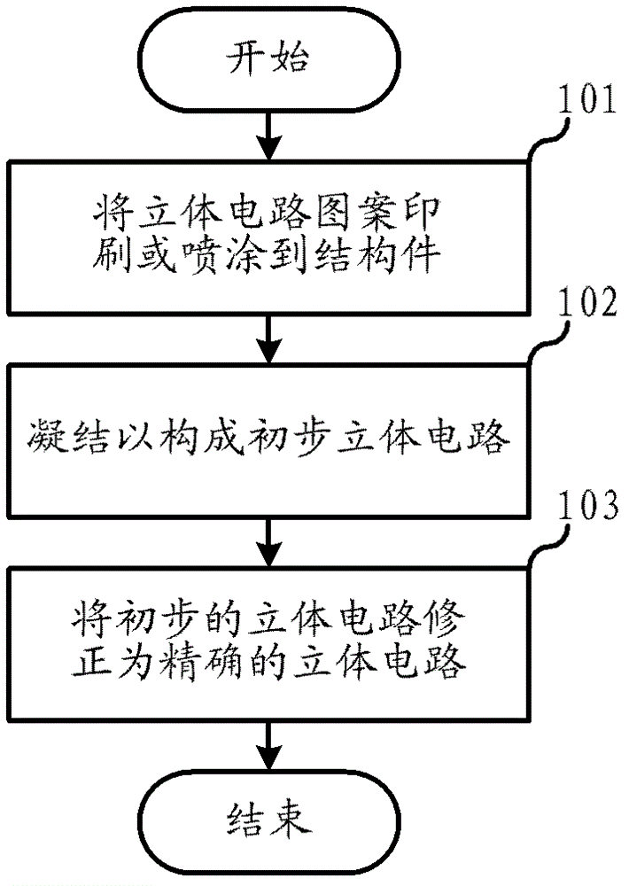
[0023] The first embodiment of the present invention relates to a method for manufacturing a three-dimensional circuit on a structural member. figure 1 It is a schematic flow chart of the manufacturing method of the three-dimensional circuit on the structure. Specifically, as figure 1 As shown, the three-dimensional circuit manufacturing method ...


PUM


Abstract

The invention relates to the field of manufacturing of circuits and discloses a three-dimensional circuit on a structure member and a manufacturing method thereof. The three-dimensional circuit can be precisely, quickly and economically formed on the structure member. The manufacturing method disclosed by the invention comprises the following steps of: printing a three-dimensional circuit pattern on the structure member by using conductive ink, or spray-coating the three-dimensional circuit pattern on the structure member by using a conductive coating, and enabling a conductive ink layer or a conductive coating layer formed after condensation to constitute a preliminary three-dimensional circuit; and using electromagnetic radiation to irradiate at least on a boundary between the part with the circuit and the part without the circuit in the three-dimensional circuit pattern so as to remove the conductive ink layer or the conductive coating layer in the irradiated region, thereby revising the preliminary three-dimensional circuit to a precise three-dimensional circuit.

Description

technical field [0001] The invention relates to the field of circuit production, in particular to a three-dimensional circuit production technology. Background technique [0002] The existing process of using conductive ink to make circuits is to form specific circuit patterns on structural parts by means of silk screen printing, pad printing or spraying, and to form circuits after being illuminated or dried. Most of these processes are used in the production of flat circuits, among which the silk screen process cannot realize three-dimensional circuits, while the spraying process needs to make complex masking tools with low resolution; the pad printing process has the opportunity to realize some three-dimensional circuits. It is to use the silicone head to absorb the conductive ink in the groove of the concave plate and then press the silicone head to the surface of the structural part, so as to transfer the conductive ink to the pre-selected area on the surface of the work...

Claims


Application Information

Patent Timeline
Patent Type & Authority Patents(China)
IPC IPC(8): H05K3/10H05K3/22H05K1/02
Inventor 王咏林金明汤毅
Owner 苏州同拓光电科技有限公司
Why Eureka
Try Eureka