One-board welding process for printed circuit board components
A welding process and assembly technology, which is applied in the field of printed board assembly single board welding process, can solve the small production batch of aerospace electronic products, the increase of single machine cost, and the inability to meet the development needs of high density and miniaturization of aerospace electronic products, etc. problem, to achieve rapid simulation optimization, miniaturization solution
- Summary
- Abstract
- Description
- Claims
- Application Information
AI Technical Summary
Problems solved by technology
Method used
Image

Examples
Embodiment 1
[0058] 1. Basic conditions
[0059] 1.1 printed board
[0060] In terms of the thickness of the printed circuit board, the limit thickness of the printed circuit board used by our company is 0.8mm and 3.0mm at present. The commonly used printed circuit board thicknesses are 1.6mm, 1.8mm, 2.0mm, 2.2mm, and 2.4mm. Therefore, the above 7 kinds of thicknesses are selected for experiments to study the influence of the thickness of the printed circuit board on the temperature of the solder joints.
[0061] In terms of the number of layers of printed circuit boards, the limit of layers used by printed circuit boards is usually 2 layers and 20 layers. The number of layers of printed circuit boards is 10 layers. Therefore, in the selection of the number of printed circuit board layers, 2-layer boards, 10-layer boards and 20-layer boards were selected for experiments to consider the contribution of the number of printed circuit board layers to the solder joint temperature.
[0062] ...
Embodiment 2
[0103] 1. Basic conditions
[0104] 1.1 printed board
[0105] To analyze the commonly used thickness of printed circuit boards, on the basis of the original first batch of printed circuit boards, carry out further impact weight subdivision tests on printed circuit boards with 4 thicknesses of 1.8mm, 2.0mm, 2.2mm, and 2.4mm.
[0106] 1.2 Solder and Flux
[0107] Same as "First Embodiment"
[0108] 1.3 Production, testing tools and equipment
[0109] Same as "First Embodiment"
[0110] 2. Process implementation steps
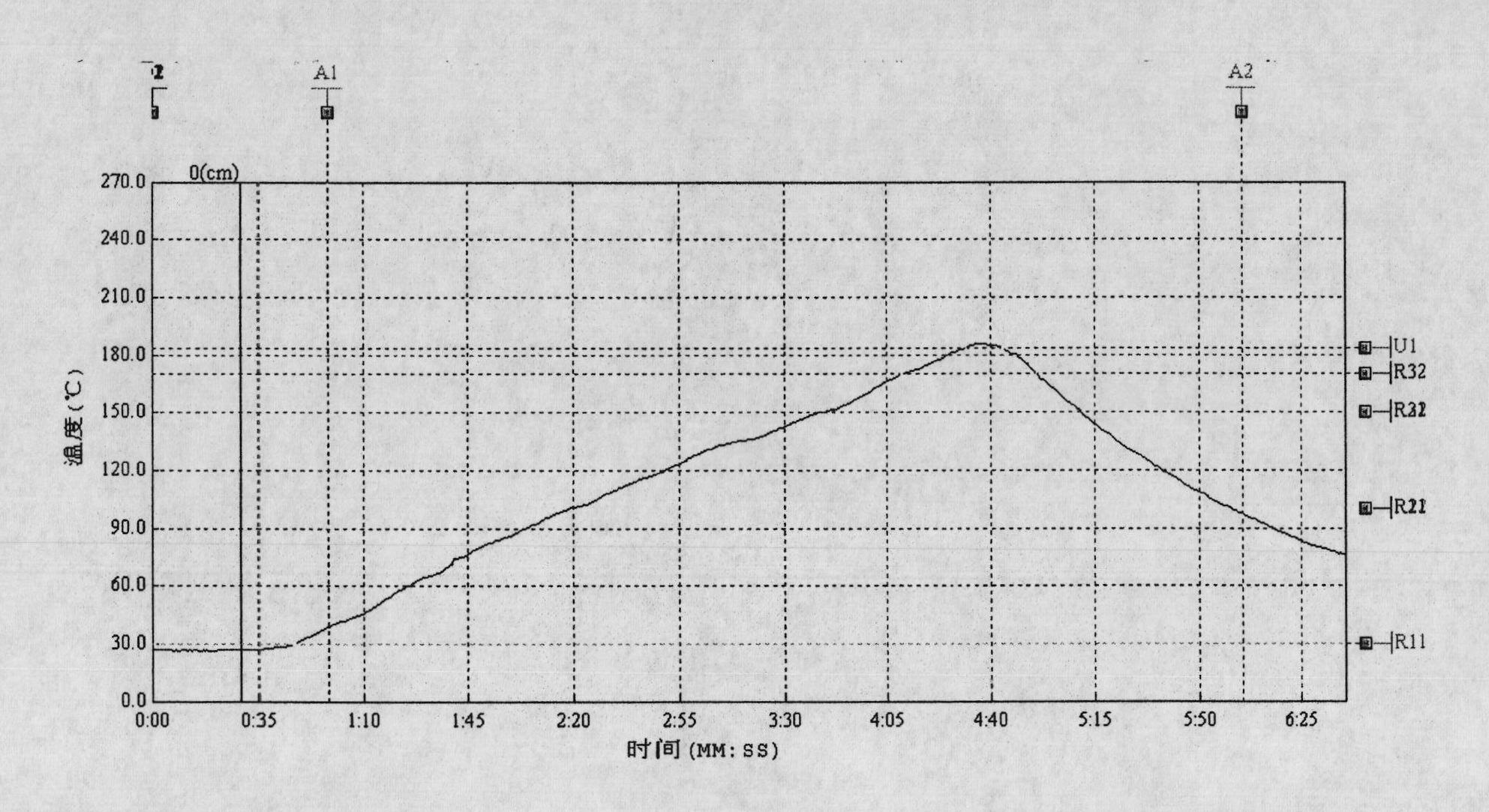
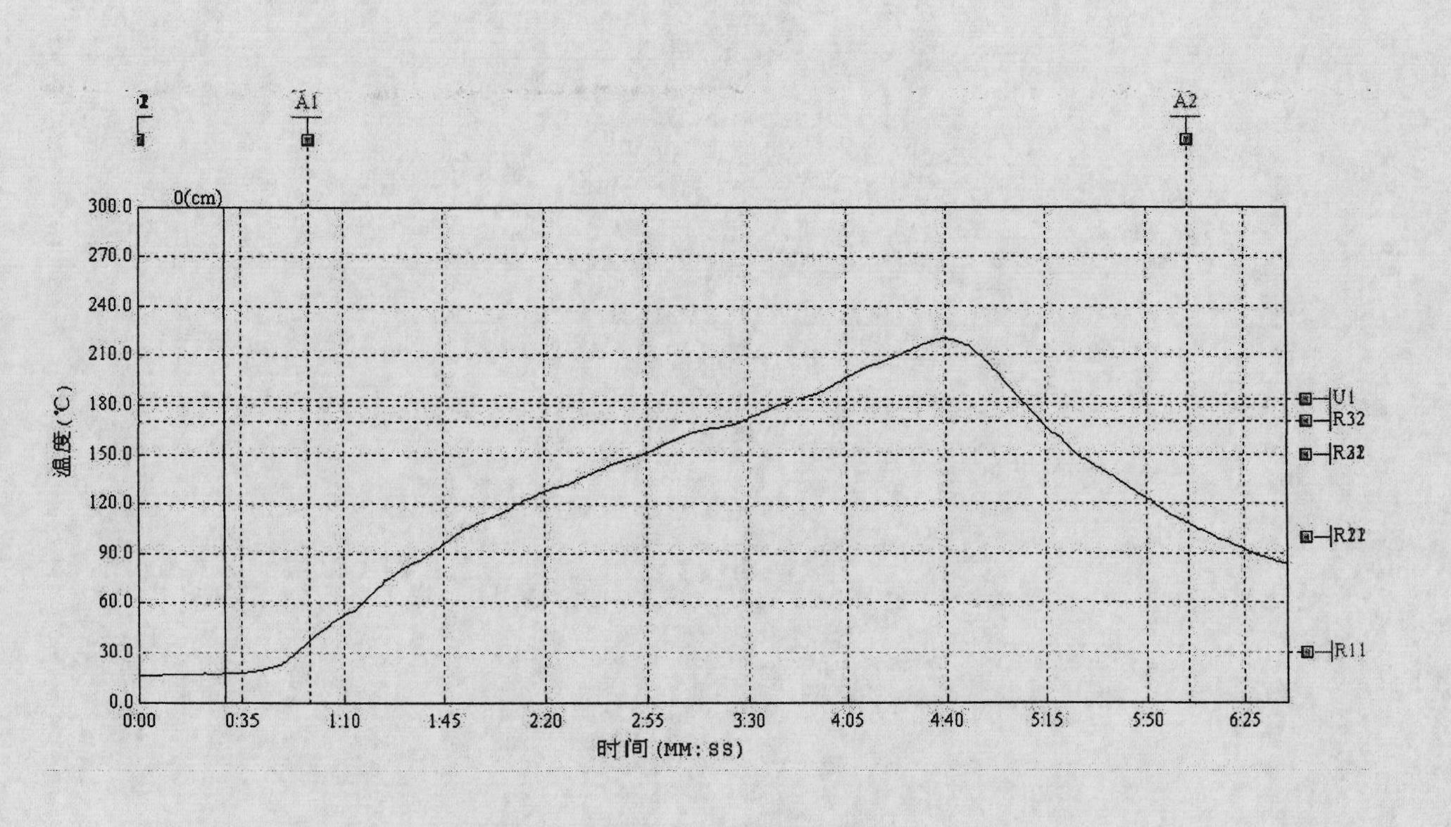
[0111] 2.1 Temperature measurement point setting
[0112] For 10-1.8, 10-2.0, 10-2.2, 10-2.4, a total of 4 kinds of printed circuit boards are installed with temperature test points. The temperature measuring point setting is the same as "the first embodiment".
[0113] 2.2 silk screen
[0114] Same as "First Embodiment"
[0115] 2.3 Reflow soldering
[0116] Same as "First Embodiment"
[0117] 2.4 Test data and analysis
[0118] A total of 36 groups ...
Embodiment 3
[0141] 1. Basic conditions
[0142] 1.1 printed board
[0143] Use 2a-3, 10m-3, 10b-3, 10-1.8, 10-2.0, 10-2.2, 10-2.4 printed circuit boards.
[0144] 1.2 Solder and Flux
[0145] Same as "First Embodiment"
[0146] 1.3 Production, testing tools and equipment
[0147] Same as "First Embodiment"
[0148] 1.4 Components
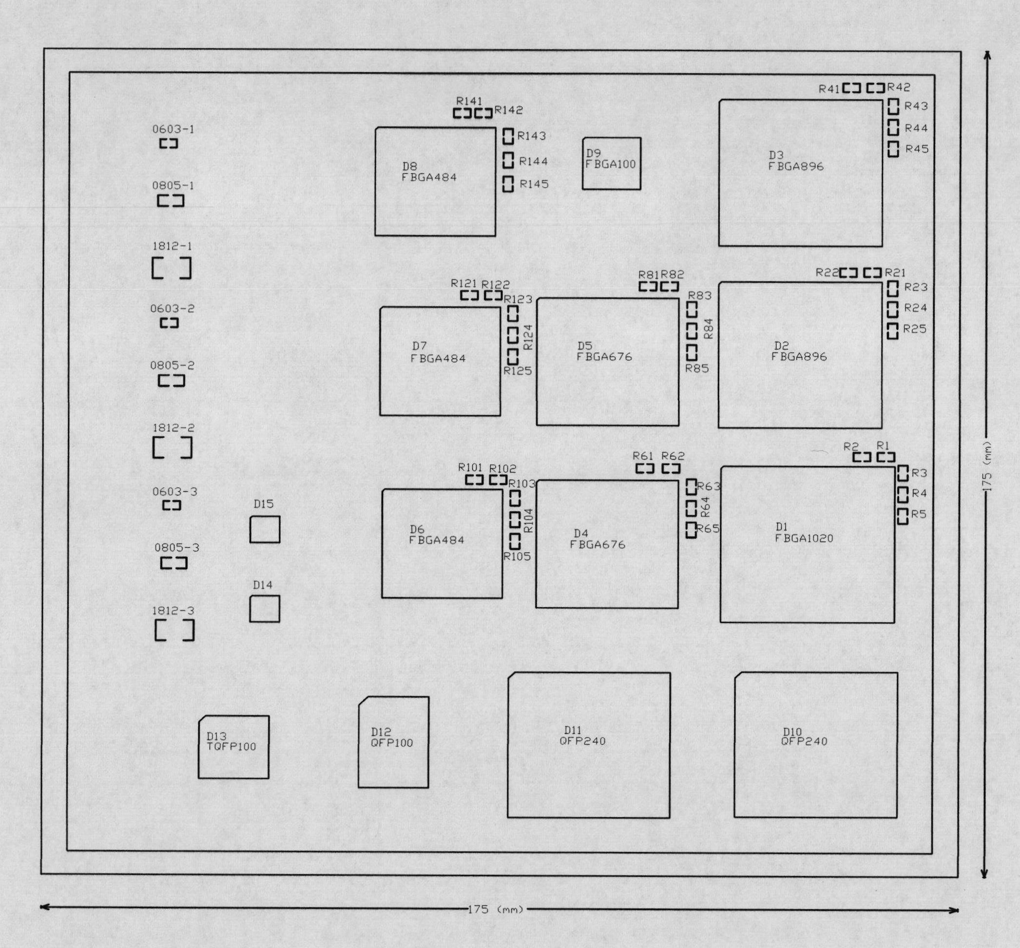
[0149] 1) Types of components (soldering terminal form)
[0150] In the selection of component types, the research group based on the typical package components commonly used in the institute, and selected resistance-capacitance components, QFP package devices, QFN package devices, and BGA package devices as test components.
[0151] There are three packages of 0603, 0805 and 1812 for the resistance and capacitance parts;
[0152] QFP selects 100-pin, 240-pin plastic and metal package devices;
[0153] QFN selects the most commonly used 20-pin plastic package device;
[0154] BGA selects 100ball, 484ball, 672ball, 896ball, 1020ball plastic packaging an...
PUM
| Property | Measurement | Unit |
|---|---|---|
| Thickness | aaaaa | aaaaa |
Abstract
Description
Claims
Application Information