Process for manufacturing sub-micrometer structure organic light emitting diode (OLED) by using porous alumina as template

A porous alumina technology, applied in the manufacture of semiconductor/solid-state devices, electrical components, electrical solid-state devices, etc., can solve the problem of difficulty in increasing the size of the mold, the poor effect of repeated use of the mold, and the inability to guarantee the embossing accuracy of hard abrasive tools and other issues to achieve the effect of improving light extraction efficiency and reducing costs

Inactive Publication Date: 2012-08-08
XI AN JIAOTONG UNIV
View PDF3 Cites 8 Cited by
  • Summary
  • Abstract
  • Description
  • Claims
  • Application Information

AI Technical Summary

Problems solved by technology

However, the use of nanoimprinting to prepare the microstructure in OLEDs still has problems such as the difficulty in increasing the size of the mold, the imprinting accuracy of commonly used hard abrasive tools cannot be guaranteed, and the effect of repeated use of molds is not good.

Method used


Image

  • Process for manufacturing sub-micrometer structure organic light emitting diode (OLED) by using porous alumina as template
  • Process for manufacturing sub-micrometer structure organic light emitting diode (OLED) by using porous alumina as template
  • Process for manufacturing sub-micrometer structure organic light emitting diode (OLED) by using porous alumina as template

Examples


Embodiment Construction

[0029] The present invention is described in further detail below in conjunction with accompanying drawing:

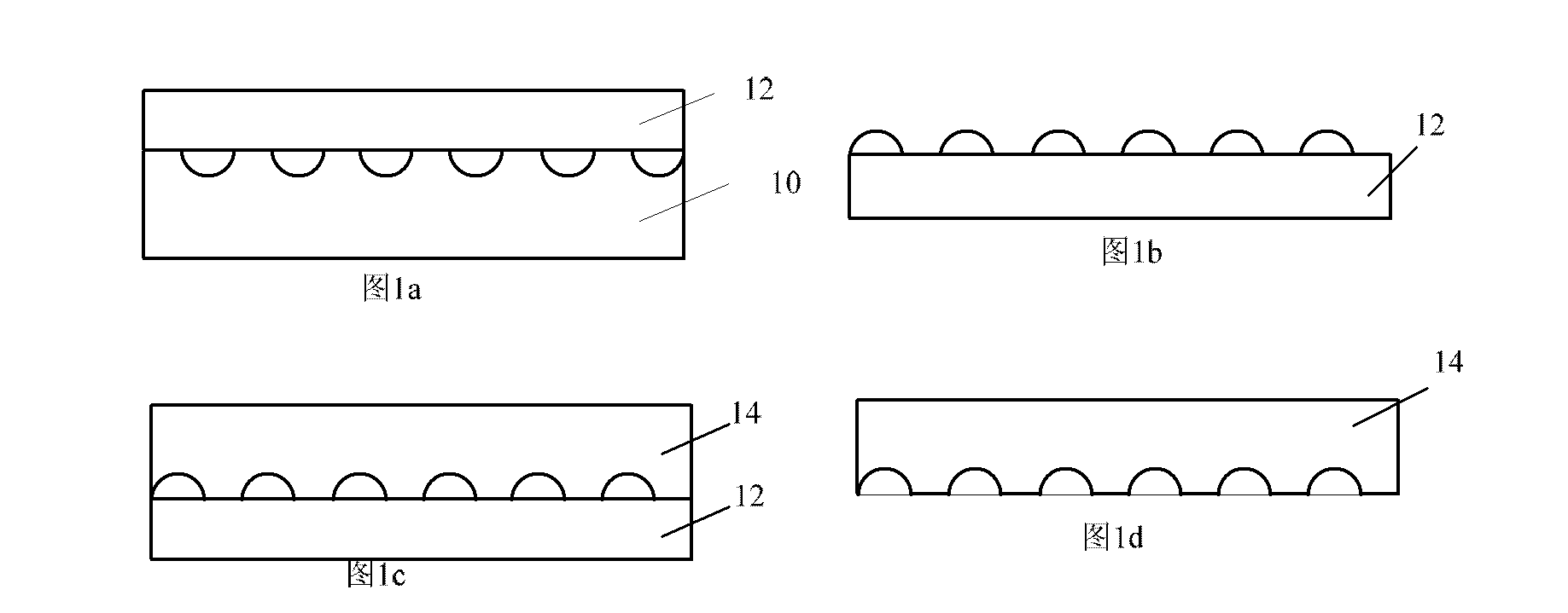
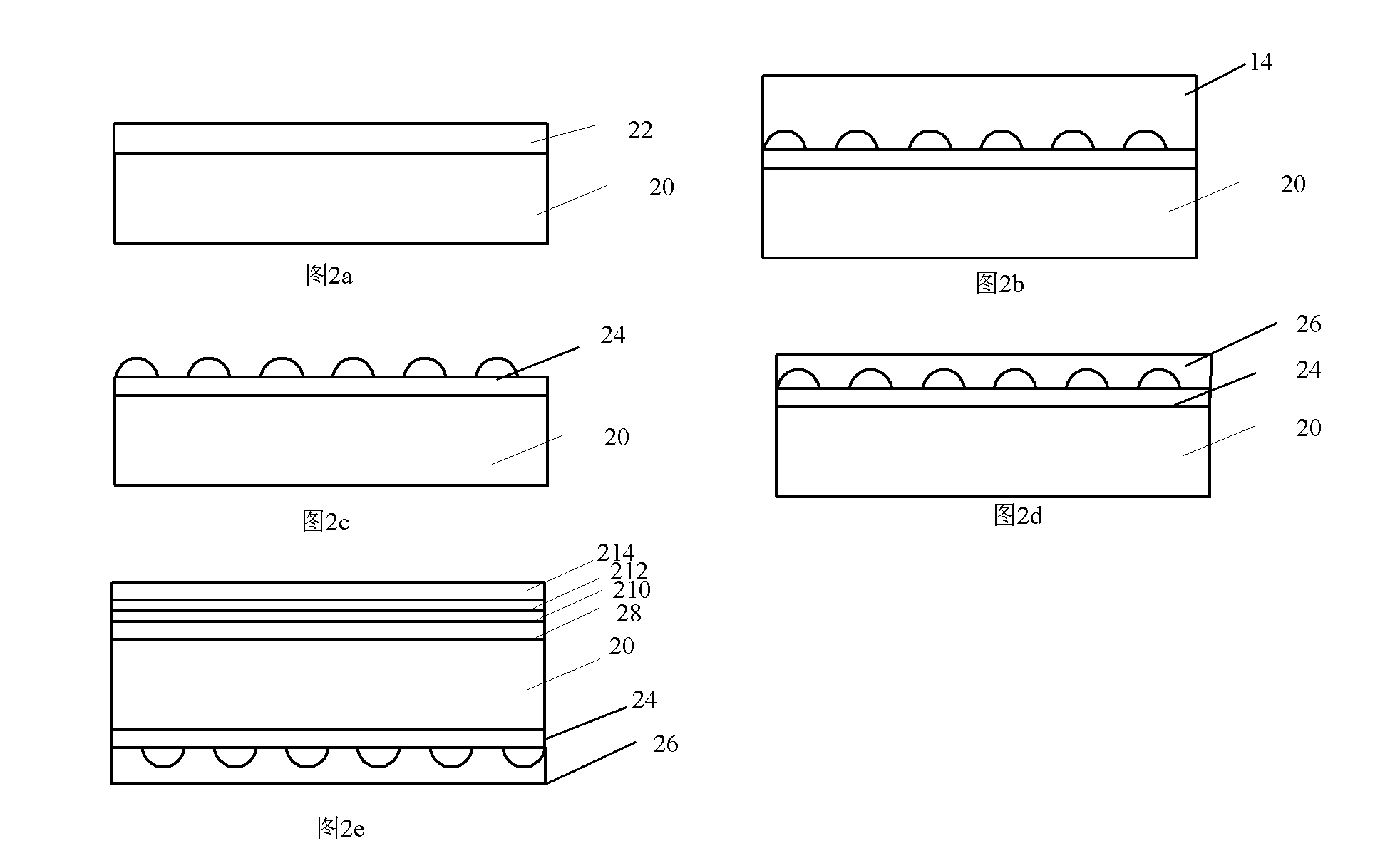
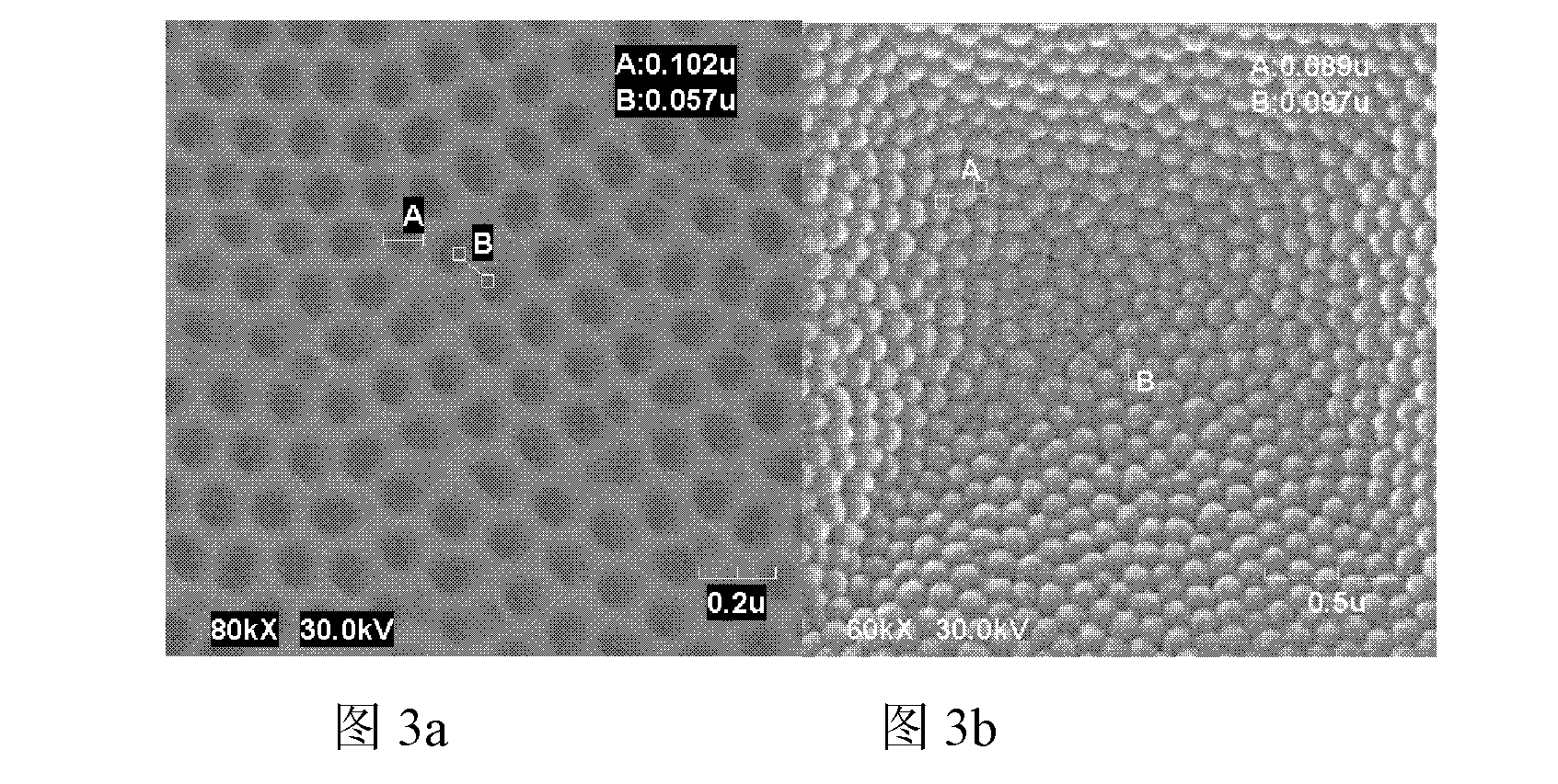
[0030] see Figure 1-4 , the process of preparing submicron-scale structures on OLEDs using porous alumina as a template in the form of ultraviolet nanoimprinting disclosed in this patent includes the following steps:

[0031] (1) if figure 1 As shown in a and 1b, the porous aluminum template is covered with PDMS, and the PDMS filler used is mixed with PDMS body and curing agent at a mass ratio of 10:1, and evenly poured on the surface of porous alumina, and then passed several times in a vacuum box. Vacuum again to remove the air bubbles in the contact surface and the solution; after the air bubbles completely disappear, put the template in an oven and bake it at 80 degrees Celsius for two hours, and after the PDMS is fully cured, peel off the PDMS from the porous alumina template;

[0032] (2) if figure 1 As shown in c and 1d, the PDMS filler is poured again on th...


PUM


Abstract

The invention discloses a process for pressing and manufacturing a sub-micrometer structure on an organic light emitting diode (OLED) by using porous alumina as a template, which comprises the steps of manufacturing a mould; imaging ultraviolet curing adhesive; manufacturing a high refraction rate media layer on the graphical ultraviolet curing adhesive by using silicon nitride produced by magnetron sputtering; and manufacturing a OLED device on an anode. The process for manufacturing the sub-micrometer structure OLED by using the porous alumina as the template reduces the cost of existing graphical technologies greatly and has potential for large-scale manufacture, so that the efficiency of OLEDs is improved remarkably, structures of organic devices on substrates are not affected, and the process is applicable to any OLED devices with light emitting structures.

Description

technical field [0001] The invention relates to an OLED manufacturing process, in particular to an OLED manufacturing process with a submicron structure. Background technique [0002] Since the first paper on OLEDs was published by Tang et al. in 1987, this new type of electronic device has attracted extensive attention from academia and industry. After more than 20 years of hard work, OLED devices have gradually entered daily life as commercial products. However, how to further improve the efficiency of the device remains to be further studied. Theoretically, the introduction of micro-nano structures into OLEDs can significantly improve its performance parameters, such as light extraction efficiency and carrier recombination rate. At present, many attempts have been made to apply micro-nano graphics in the OLED manufacturing process. However, most of the current preparation processes for submicron structures use electron beam direct writing, focused ion beam direct writi...

Claims


Application Information

Patent Timeline
Patent Type & Authority Applications(China)
IPC IPC(8): H01L51/56
Inventor 王莉丁玉成罗钰魏慧芬卢秉恒
Owner XI AN JIAOTONG UNIV
Why Eureka
Try Eureka