Defect width calibration standardizing system and method in optical surface defect dark field detection
A technology for optical surface and dark field detection, which is applied in the direction of optical testing for flaws/defects, etc. It can solve the problems of difficult and large-diameter component detection, slow detection time, and inability to accurately calibrate defects, etc., to achieve large detection range and high The effect of detection speed
- Summary
- Abstract
- Description
- Claims
- Application Information
AI Technical Summary
Problems solved by technology
Method used
Image

Examples
Embodiment
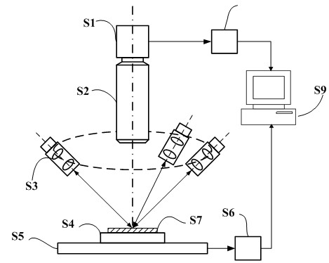
[0035] Schematic diagram of standardization system for defect width calibration in dark field detection of optical surface defects. figure 1 shown. Use the ring lighting LED light source to illuminate the calibration plate located on the working platform, use a high-resolution CCD with a resolution of 2048×2048, observe the calibration plate and collect images through a 1X-16X continuous zoom microscope, and form a microscope dark field imaging. The working platform where the quartz calibration plate is located is moved by a one-dimensional guide rail with a precision of 1 μm controlled by a computer, and the scanning of the sub-aperture of the calibration plate is realized.
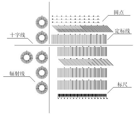
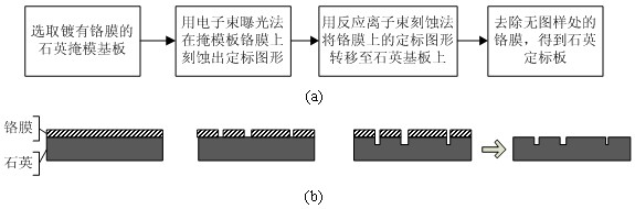
[0036] According to the above steps, first make a quartz calibration plate engraved with a series of standard graphics. The completed quartz calibration plate is sampled, and a group of calibration lines on a calibration plate is selected to measure the width of the calibration line with a scanning ele...
PUM
 Abstract
Description
Claims
Application Information
 - R&D
- Intellectual Property
- Life Sciences
- Materials
- Tech Scout
- Unparalleled Data Quality
- Higher Quality Content
- 60% Fewer Hallucinations
Browse by: Latest US Patents, China's latest patents, Technical Efficacy Thesaurus, Application Domain, Technology Topic, Popular Technical Reports.
© 2025 PatSnap. All rights reserved.Legal|Privacy policy|Modern Slavery Act Transparency Statement|Sitemap|About US| Contact US: help@patsnap.com