Array substrate and preparation method thereof

An array substrate and substrate technology, applied in the field of array substrate and its preparation, can solve problems such as unstable electrical conductivity of contact holes, damage to the surface of the medium, complex patterning process, etc., achieve reliable and stable electrical conductivity, ensure film quality, and simplify preparation The effect of craft

Active Publication Date: 2012-08-15
BOE TECH GRP CO LTD +1
View PDF4 Cites 5 Cited by
  • Summary
  • Abstract
  • Description
  • Claims
  • Application Information

AI Technical Summary

Problems solved by technology

[0004] Since the contact holes above the gate electrode metal layer and the contact holes above the data line metal layer are etched in the same patterning process, the film quality and film thickness of the dielectric above the gate electrode metal layer and the data line metal layer are different. The same, so this kind of patterning process is complicated, and the depth of etching is not easy to control. On the one hand, it is easy to cause over-etching or not penetrating; A chamfer is formed between the metal layers of the data line, and when the transparent conductive layer 11 covers two contact holes with different depths, it is easy to cause a crossover, such as figure 2 As shown; moreover, using this patterning process to etch a contact hole on the medium will cause damage to the surface of the medium; therefore, the conductivity of the contact hole obtained using this patterning process is unstable, which will directly have a negative impact on the display performance of the display

Method used


Image

  • Array substrate and preparation method thereof
  • Array substrate and preparation method thereof
  • Array substrate and preparation method thereof

Examples


Embodiment Construction

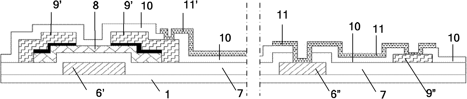
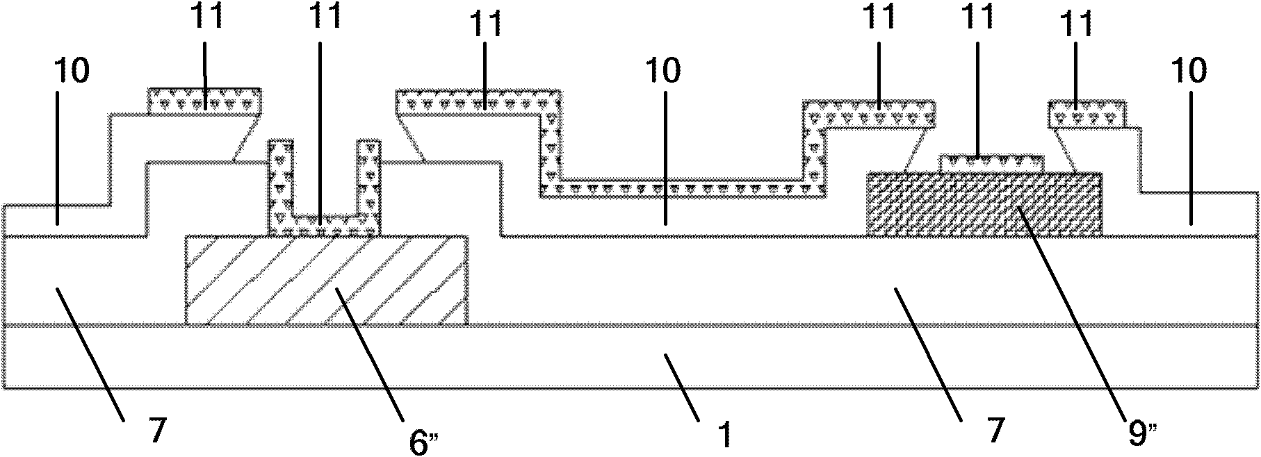
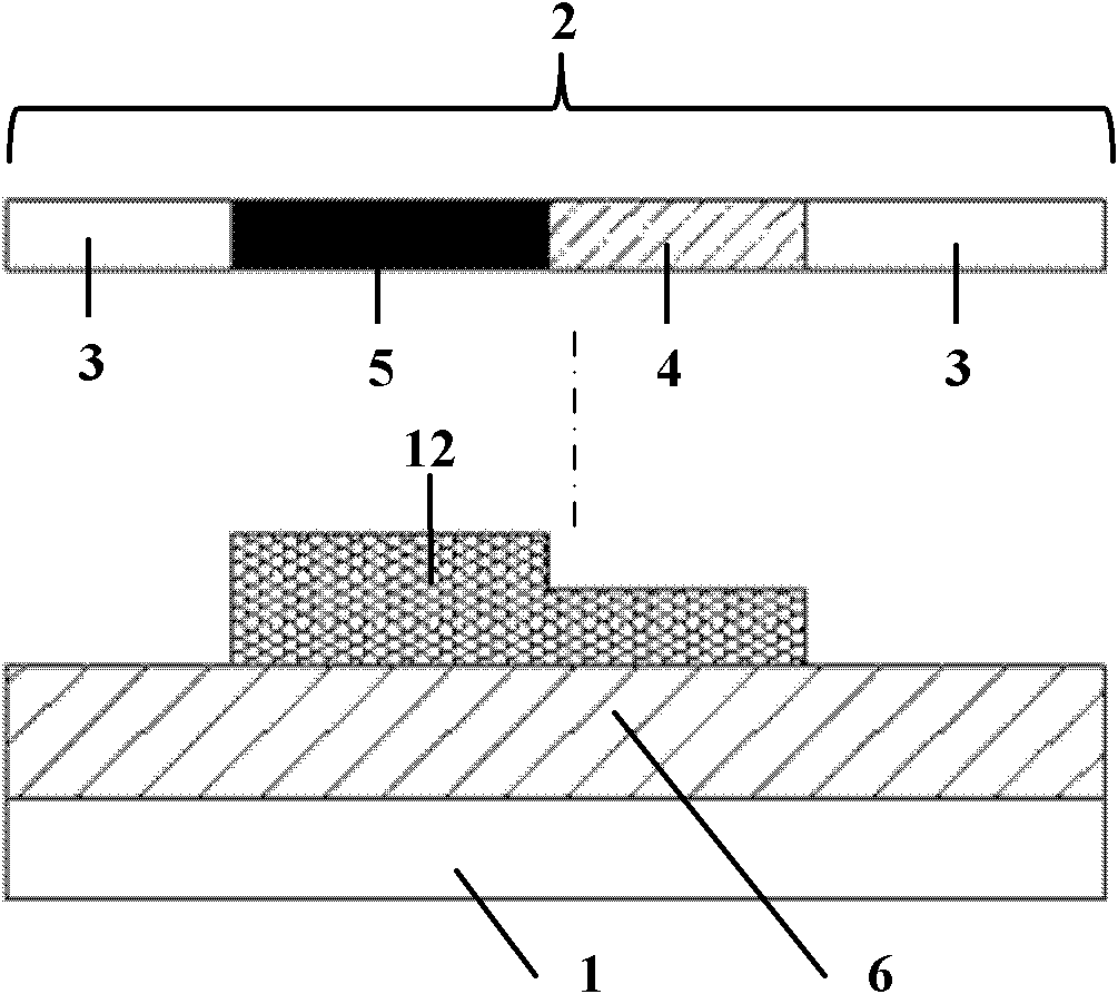
[0041]Those skilled in the art know that in the process of manufacturing a TFT-LCD, it is necessary to perform a patterning process on the film layer according to product design requirements to obtain the required film morphology. That is, apply photoresist on the substrate after film formation, and expose the substrate with a mask plate with the target pattern. The light on the part without pattern on the mask plate can completely pass through, and the properties of the photoresist after being irradiated by light Changes occur, and in subsequent development, the photoresist that is irradiated by light (referring to positive photoresist) is dissolved in the developer solution or the photoresist that is not irradiated by light (referring to negative photoresist) is dissolved in the developer solution , and then etch away the film layer without photoresist protection, and finally peel off the photoresist to form a film layer on the substrate with the same shape as the target patt...


PUM


Abstract

The invention discloses an array substrate and a preparation method thereof. The array substrate comprises a substrate, gate electrodes, a gate insulating layer, a silicon island, source drain electrodes, a passivation layer and pixel electrodes, wherein two layers of conductive structures separated from each other through insulating media are connected by virtue of a connecting part, and the conductive structure below the connecting part and the insulating media is formed through a primary composition technology with a halftone or grey tone. According to the invention, the preparation technology of the array substrate is simplified.

Description

technical field [0001] The invention relates to the technical field of microfabrication in the semiconductor industry, in particular to an array substrate and a preparation method thereof. Background technique [0002] Thin-film transistor-liquid crystal display, an optoelectronic product that integrates large-scale semiconductor integrated circuits and flat-panel light source technology with thin-film transistors as control elements and liquid crystals as the medium, has become a new generation of mainstream displays. [0003] The display quality and overall performance of thin film transistor liquid crystal displays are largely affected by materials, device structures and processes. In the preparation process of the array substrate of the thin film transistor liquid crystal display, on the one hand, it is necessary to connect the display pixel area with the peripheral driving circuit; Interconnection between layers. In this paper, the conductive layer refers to the gate...

Claims


Application Information

Patent Timeline
Patent Type & Authority Applications(China)
IPC IPC(8): H01L27/12H01L21/84H01L21/768G02F1/1362G02F1/1368
CPCH01L27/1288
Inventor 李坤玄明花高永益
Owner BOE TECH GRP CO LTD
Why Eureka
Try Eureka