Semiconductor structure and preparation method of semiconductor structure

A type of semiconductor technology, used in semiconductor/solid-state device manufacturing, semiconductor devices, electrical components, etc., can solve problems such as structural design and simulation difficulties, and achieve the effect of simple structure, improved breakdown voltage, and simplified device design.

Inactive Publication Date: 2012-08-15
SHANGHAI HUAHONG GRACE SEMICON MFG CORP
View PDF3 Cites 2 Cited by
  • Summary
  • Abstract
  • Description
  • Claims
  • Application Information

AI Technical Summary

Problems solved by technology

[0005] In the field limit ring structure, it is necessary to strictly control the doping concentration and diffusion depth of the doped region, as well as the distance between the main junction and the field

Method used


Image

  • Semiconductor structure and preparation method of semiconductor structure
  • Semiconductor structure and preparation method of semiconductor structure
  • Semiconductor structure and preparation method of semiconductor structure

Examples


Embodiment Construction

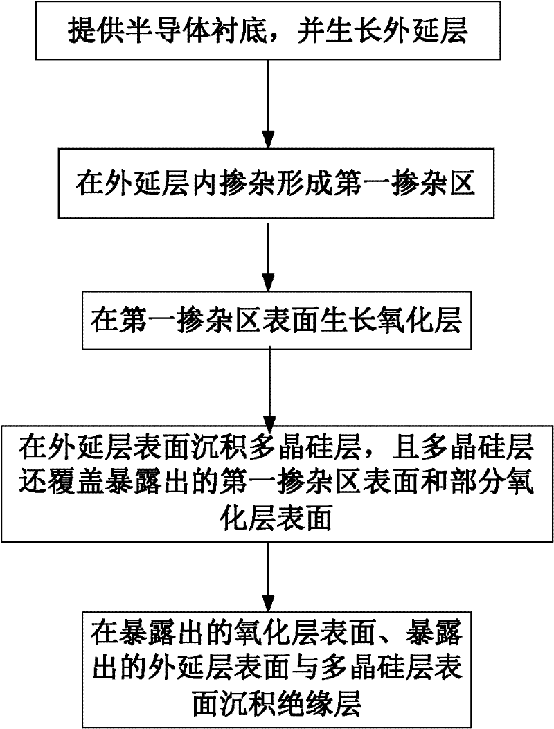
[0028] In order to make the object, technical solution and advantages of the present invention clearer, the present invention will be further described in detail below in conjunction with the accompanying drawings.

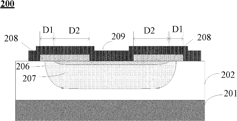
[0029] figure 2 It is a schematic diagram of a cross-sectional structure of a semiconductor structure provided by the present invention.

[0030] Such as figure 2 As shown, the semiconductor structure 200 includes: a semiconductor substrate 201 having a first semiconductor type; an epitaxial layer 202 covering the surface of the semiconductor substrate 201; a first diffusion region 206 having a second semiconductor type located in the epitaxial layer 202; An oxide layer 207 on the surface of the diffusion region 206, whose surface is substantially flat with the surface of the epitaxial layer; a polysilicon layer 208 on the surface of the epitaxial layer 202, and the polysilicon layer 208 also covers part of the surface of the oxide layer 207 and the exposed fir...


PUM

PropertyMeasurementUnit
Sizeaaaaaaaaaa
Sizeaaaaaaaaaa
Thicknessaaaaaaaaaa

Abstract

The invention relates to a semiconductor structure and a preparation method of the semiconductor structure and belongs to the field of a semiconductor device. The semiconductor structure comprises a semiconductor substrate, an epitaxial layer, a first diffusion region, an oxidation layer, a polycrystalline silicon layer and an insulation layer, wherein the semiconductor substrate has the first semiconductor type, the epitaxial layer is covered on the surface of the semiconductor substrate, the first diffusion region is positioned in the epitaxial layer and has the second semiconductor type, the oxidation layer is arranged on the surface of the first diffusion surface, and in addition, the surface of the oxidation layer is basically aligned with the surface of the epitaxial layer, the polycrystalline silicon layer is positioned on the surface of the epitaxial layer and covers the partial oxidation layer surface, the partial epitaxial layer surface and the exposed first diffusion surface, and the insulation layer is positioned on the exposed oxidation layer surface, the exposed epitaxial surface and the polycrystalline silicon layer surface. Through the adoption of the RESURF technology, a low-doping first doping region is arranged in the semiconductor structure, and during the PN junction reverse deflection, the PN junction can realize the uniform load bearing through the RESURF technology. In addition, the thick oxidation layer can also be used for effectively improving the breakdown voltage of the PN junction. Meanwhile, the semiconductor structure provided by the invention has the advantages that the structure is simple, and the process is simple and convenient.

Description

technical field [0001] The invention relates to a semiconductor structure, in particular to the structure of a protection ring, and belongs to the technical field of semiconductors. Background technique [0002] Modern high-voltage power semiconductor devices are more and more widely used due to their high operating frequency, fast switching speed, and high control efficiency. However, due to the planar terminal structure used in the semiconductor process, the depth of the junction is shallow and the edge of the junction is bent, which reduces the withstand voltage. , Poor stability, and the device is easily damaged. In order to improve the device withstand voltage and withstand voltage stability, measures are usually taken at the device boundary, that is, terminal protection technology to reduce the surface electric field intensity and increase the breakdown voltage of the PN junction of the power device. [0003] The commonly used terminal structures are as follows: Field...

Claims


Application Information

Patent Timeline
IPC IPC(8): H01L29/06H01L21/02
Inventor 王颢克里斯吴小利
Owner SHANGHAI HUAHONG GRACE SEMICON MFG CORP
Why Eureka
Try Eureka