

Crystalline silicon solar Metal Wrap Through (MWT) battery and manufacturing method thereof
A production method and solar energy technology, applied in circuits, photovoltaic power generation, electrical components, etc., can solve problems such as hidden cracks, fragments, and increased defective products, and achieve the effects of easy interconnection, reduced equipment investment, and accelerated industrialization
- Summary
- Abstract
- Description
- Claims
- Application Information
AI Technical Summary
Problems solved by technology
Method used
Image

Examples
Embodiment 1
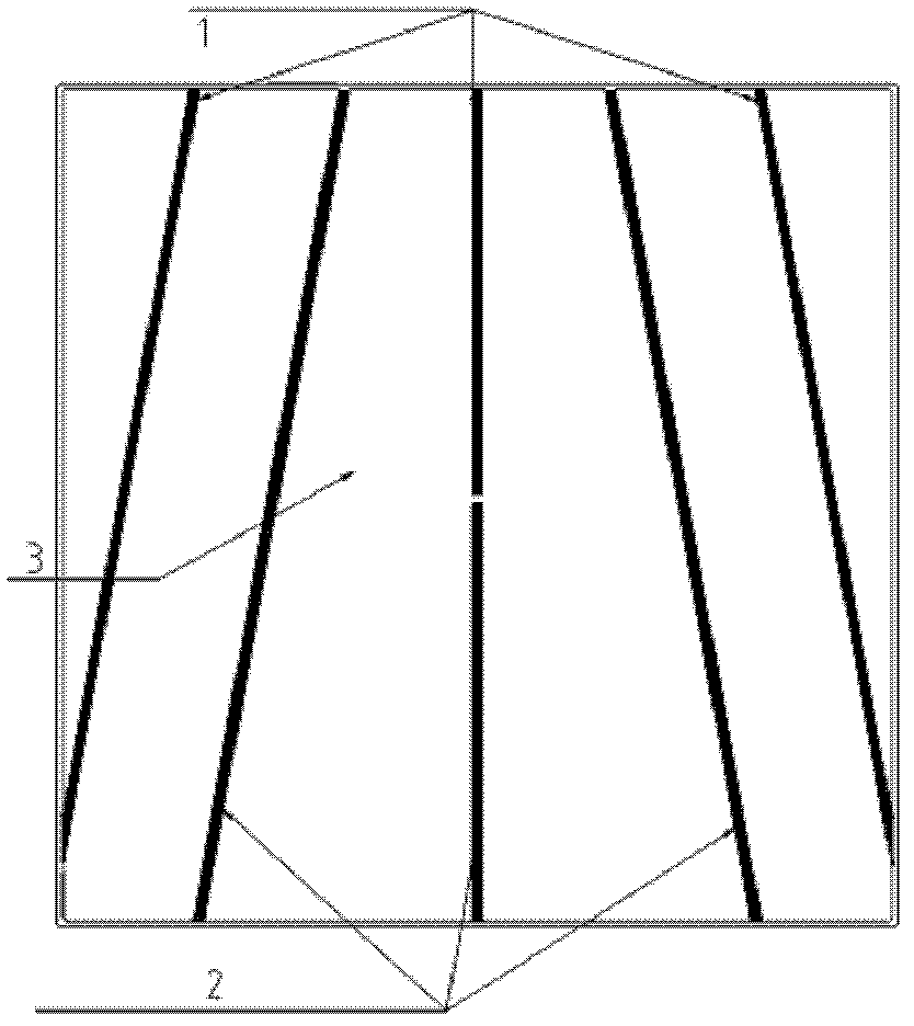
[0033] Embodiment 1: as figure 1 , figure 2 , image 3 , Figure 4 , Figure 5 as shown,
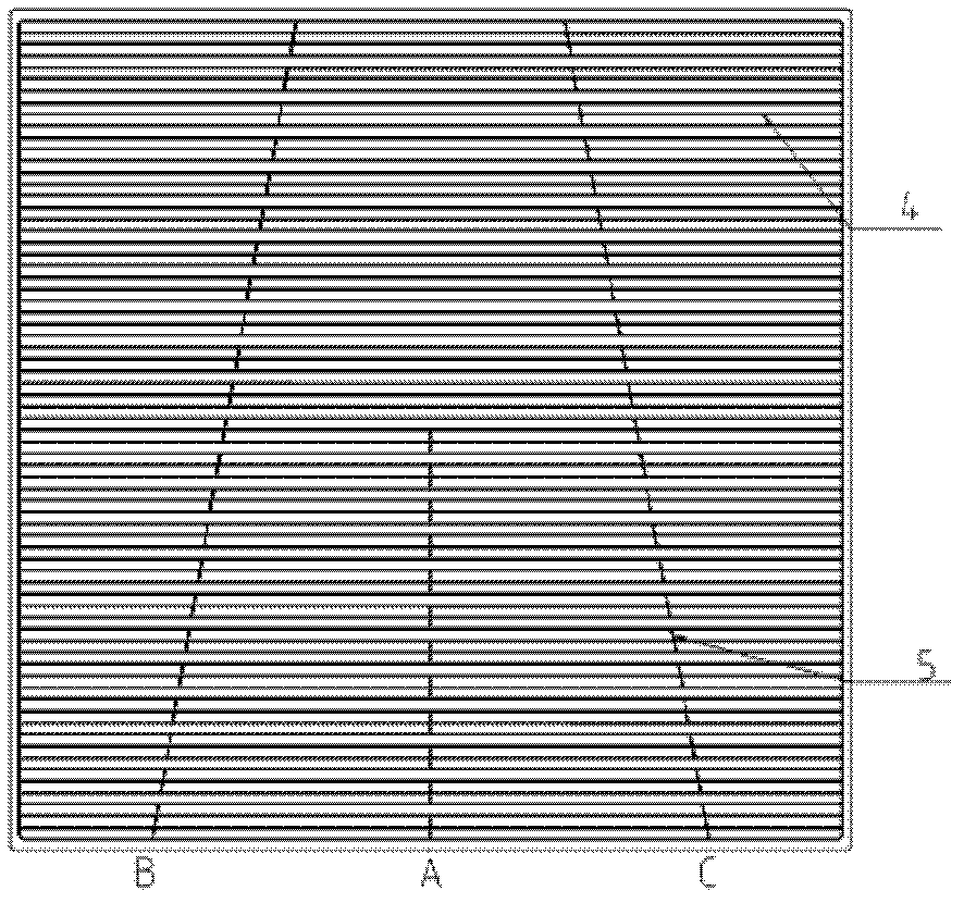
[0034] A method for manufacturing a crystalline silicon solar MWT cell, comprising the following steps: firstly, a figure-splayed distribution of laser holes is drilled on a bare silicon wafer, and then the battery sheet process is performed: texturing, diffusion, PSG removal, PECVD, screen printing, sintering, Laser isolation. The steps of the screen printing section are: ① Simultaneously print the back positive electrode (1) and the back negative electrode (2); ② Print the back electric field (3); ③ Simultaneously print the front grid lines (4) and the front hole filling grid lines (5).
[0035] 1. The biggest feature of the punching pattern is the figure-eight shape, such as figure 2 As shown, about 10 holes in group A in the middle are distributed vertically downward from the center of the silicon wafer, and about 25 holes in groups C and B are located in a figure-eight shape...
Embodiment 2
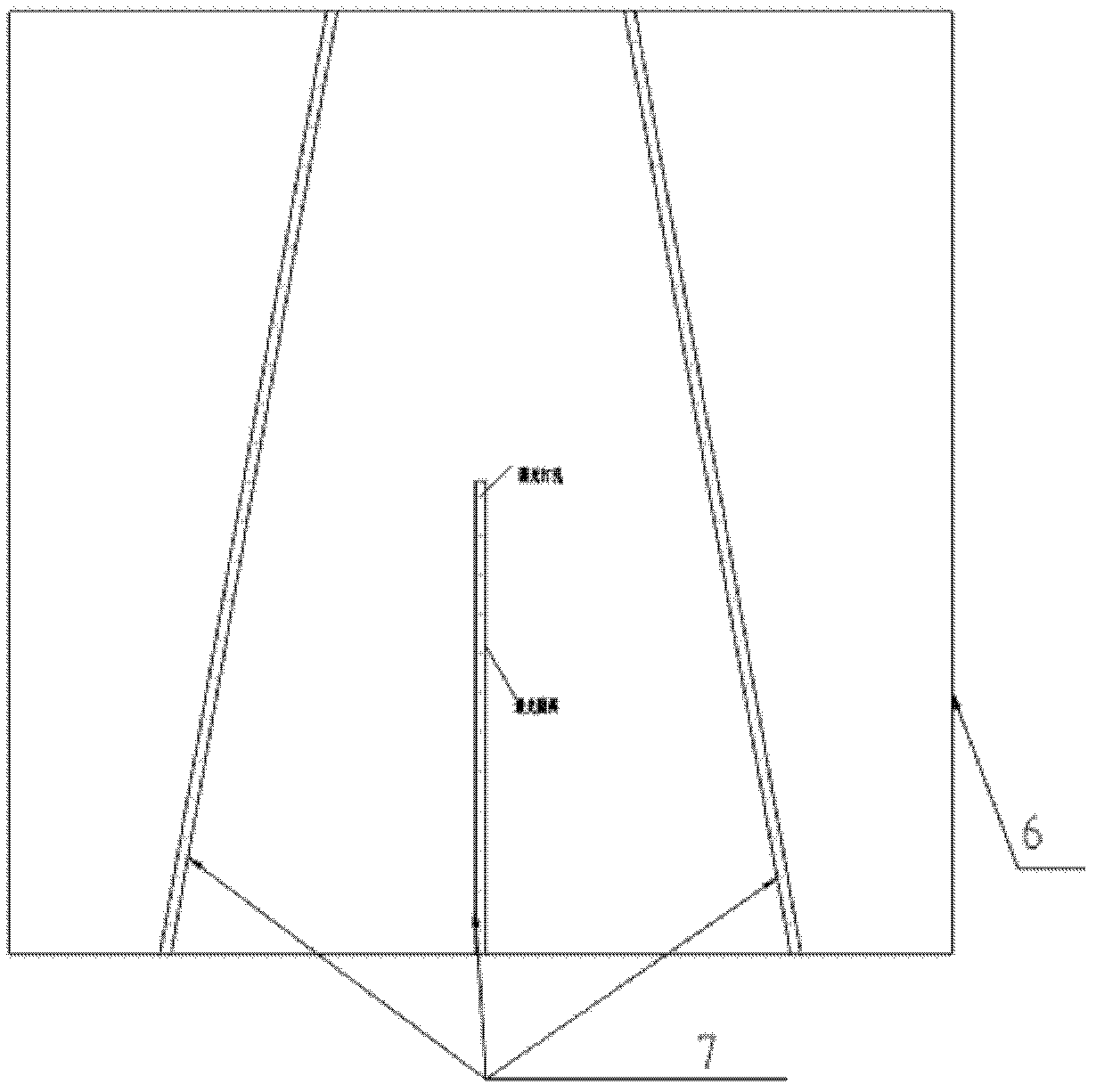
[0043] A crystalline silicon solar MWT battery and its manufacturing method. The MWT battery realizes the conduction of the upper and lower perforated electrodes through a unique pattern of eight-shaped distribution of holes. Diffusion, PSG removal, PECVD, screen printing, sintering, laser isolation. The steps of the screen printing section are: ① Simultaneously print the back positive electrode (1) and the back negative electrode (2); ② Print the back electric field (3); ③ Simultaneously print the front grid lines (4) and the front hole filling grid lines (5). The interconnection of the cells is all realized on the back side, using the traditional welding process, from the back negative electrode (or back negative electrode) of the battery piece 1 to the back negative electrode (or back negative electrode) of the battery piece 2. The high compatibility of traditional component technology solves the problem of high component cost of MWT batteries in the current market. The sh...
PUM
| Property | Measurement | Unit |
|---|---|---|
| Width | aaaaa | aaaaa |
| Width | aaaaa | aaaaa |
| Width | aaaaa | aaaaa |
Abstract
Description
Claims
Application Information