Transparent conductive laminate, method for producing same, and electrostatic capacitance type touch panel

A transparent conductive layer and transparent conductive technology, which is applied in the direction of cable/conductor manufacturing, conductive layer on insulating carrier, chemical instruments and methods, etc., can solve the problems of reduced visibility, increased manufacturing process, complicated manufacturing process, etc. Achieve high visibility and easy alignment

Inactive Publication Date: 2012-08-15
TOPPAN PRINTING CO LTD
View PDF9 Cites 15 Cited by
  • Summary
  • Abstract
  • Description
  • Claims
  • Application Information

AI Technical Summary

Problems solved by technology

In addition, when an optical adjustment layer is formed in addition to the transparent conductive layer as in Patent Document 6 in order to solve the problem of deterioration in visibility, it is necessary to further increase the number of manufacturing steps, so that the manufacturing steps become more complicated.

Method used


Image

  • Transparent conductive laminate, method for producing same, and electrostatic capacitance type touch panel
  • Transparent conductive laminate, method for producing same, and electrostatic capacitance type touch panel
  • Transparent conductive laminate, method for producing same, and electrostatic capacitance type touch panel

Examples


Embodiment 1

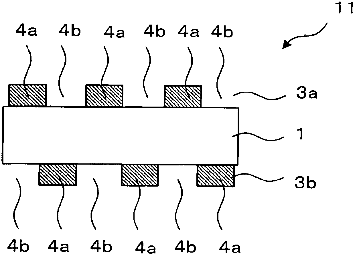
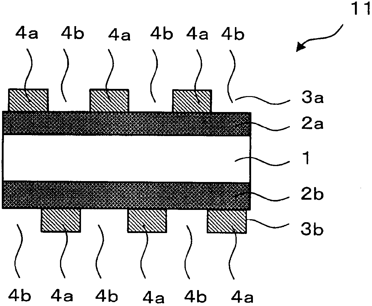
[0115] A polyethylene terephthalate film (manufactured by Toray Co., Ltd., thickness: 100 μm) having an ultraviolet absorbing function was used as a transparent substrate, and a resin layer of the following composition was coated on both sides of the transparent substrate using a micro-gravure coater The coating liquid for formation was dried at 60° C. for 1 minute, and cured by ultraviolet rays to form a resin layer.

[0116] [Composition of Coating Liquid for Resin Layer Formation]

[0117] Resin: 100 parts by weight of Ziguang UV-7605B (manufactured by Nippon Synthetic Chemicals Co., Ltd.)

[0118]Initiator: 4 parts by weight of Irgacyua 184 (manufactured by Chiba Japan Co., Ltd.)

[0119] Solvent: 100 parts by weight of methyl acetate

[0120] Next, on both surfaces of the resin layer formed on both surfaces of the transparent substrate, ITO was formed into a film of 30 nm by a sputtering method to form a transparent conductive layer. Then, use such as Figure 12 and ...

Embodiment 2

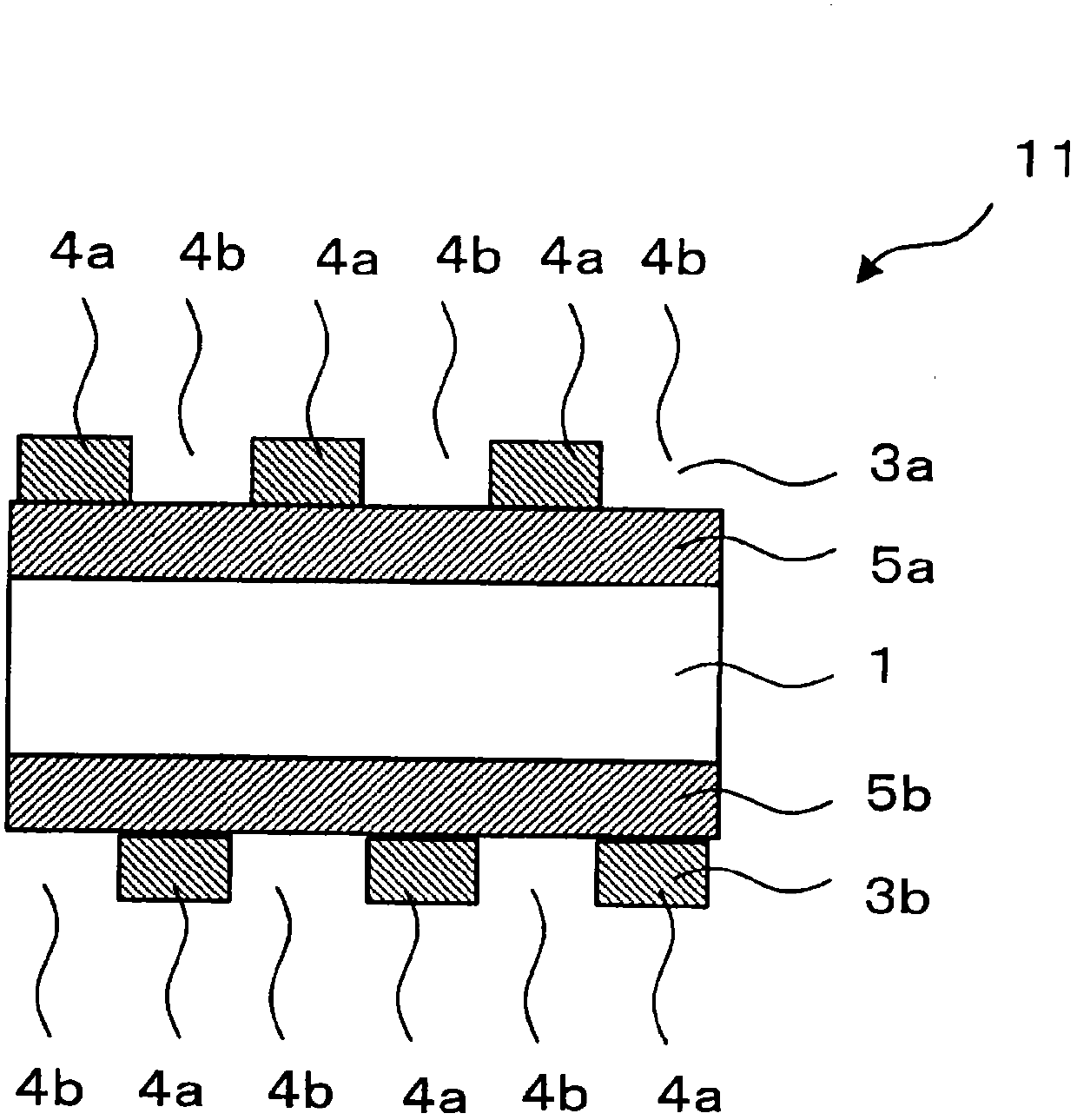
[0126] In addition to using a polyethylene terephthalate film (manufactured by Toray Co., Ltd., thickness: 100 μm) that does not have an ultraviolet absorbing function as a transparent substrate, and containing 0.5 parts by weight of a triazine-based ultraviolet absorbing film in the coating liquid for forming a resin layer, Agent (2-{4-[(2-hydroxy-3-tridecyloxypropyl)oxy]-2-hydroxyphenyl}-4,6-bis(2,4-dimethylphenyl) -1,3,5-triazine), using the same conditions and methods as in Example 1, a conductive pattern region and a nonconductive pattern region were formed on the transparent conductive layer.


PUM

PropertyMeasurementUnit
thicknessaaaaaaaaaa
thicknessaaaaaaaaaa
transmittivityaaaaaaaaaa

Abstract

Provided are a transparent conductive laminate, a method for producing the same, and an electrostatic capacitance type touch panel, wherein fine patterns having different shapes can be formed on opposite sides of a substrate at the same time during a short production step, and positioning of the fine patterns is easy. A transparent conductive laminate (11) comprises a transparent substrate layer (1), and a first transparent conductive layer (1a) and a second transparent conductive layer (1b) formed on the opposite sides of the transparent substrate layer (1), the first transparent conductive layer (1a) having a first conductive pattern area (4a) and a first nonconductive pattern area (4b), and the second transparent conductive layer (1b) having a second conductive pattern area (4a) and a second nonconductive pattern area (4b), wherein at least one layer formed between the first transparent conductive layer (1a) and the second transparent conductive layer (1b) functions to absorb light.

Description

technical field [0001] The present invention relates to a transparent conductive laminate and a method for producing the transparent conductive laminate. Background technique [0002] In recent years, transparent touch panels as input devices have been mounted on displays of various electronic devices. As the system of the touch panel, a resistive film type, an electrostatic capacity type, etc. are mentioned. In particular, the capacitive type is capable of multi-touch, so it is widely used in applications such as mobile devices. [0003] Capacitive touch panels use a patterned transparent conductive layer. As a method of forming a pattern on this transparent conductive layer, there are methods using photolithography for patterning using a resist described in Patent Documents 1 to 3, for example. As another method, there is a method of using an indium compound having a functional group or a site that reacts to light and a tin compound having the same functional group or s...

Claims


Application Information

Patent Timeline
Patent Type & Authority Applications(China)
IPC IPC(8): B32B7/02G06F3/041G06F3/044H01B5/14H01B13/00
CPCB32B7/12B32B27/08B32B2255/10B32B2255/20B32B2255/26B32B2255/28B32B2307/202B32B2307/412B32B2457/16B32B2457/208B32B2509/00Y10T428/24942G06F3/0445G06F3/041G06F3/044H03K17/962B32B7/025
Inventor 小林裕
Owner TOPPAN PRINTING CO LTD
Why Eureka
Try Eureka